Features: Isolation Test Voltage: To 3.5 kV rmsFive Isolated Logic Lines: Available in Six I/O ConfigurationsLogic Signal Bandwidth: 20 MHz (min)CMV Transient Immunity: 10 kV/ms minWaveform Edge Transmission Symmetry: 61 nsField and System Output Enable/Three-State FunctionsPerformance Rated Over ...
AD261: Features: Isolation Test Voltage: To 3.5 kV rmsFive Isolated Logic Lines: Available in Six I/O ConfigurationsLogic Signal Bandwidth: 20 MHz (min)CMV Transient Immunity: 10 kV/ms minWaveform Edge Tra...
SeekIC Buyer Protection PLUS - newly updated for 2013!
268 Transactions
All payment methods are secure and covered by SeekIC Buyer Protection PLUS.
Parameter | Conditions | Min | Typ | Max | Unit |
Supply Voltage (+5 V dcSYS & FLD) | 0.5 | +6.0 | V | ||
DC Input Voltage (VIN MAX) | Referred to +5 V dcSYS & FLD and 5 V RTNSYS & FLD Respectively | 0.5 | +0.5 | V | |
DC Output Voltage (VOUT MAX) | Referred to +5 V RTNSYS & FLD and 5 V dcSYS & FLD Respectively | 0.5 | +0.5 | V | |
Clamp Diode Input Current (IIK) | For VI < 0.5 V or VI > 5 V RTNSYS & FLD +0.5 V | 25 | +25 | mA | |
Clamp Diode Output Current (IOK) | For VO < 0.5 V or VO > 5 V RTNSYS & FLD +0.5 V | 25 | +25 | mA | |
Output DC Current, per Pin (IOUT) | 25 | +25 | mA | ||
DC Current, VCC or GND (ICC or IGND) | 50 | +50 | mA | ||
Storage Temperature (TSTG) | 40 | +85 | |||
Lead Temperature (Soldering, 10 sec) | +300 | ||||
Electrostatic Protection (VESD) | Per MIL-STD-883, Method 3015 | 4.5 | 5 | kV |
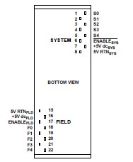
The AD261 is designed to isolate five digital control signals to/from a microcontroller and its related field I/O components.Six models allow all I/O combinations from five input lines to five output lines, including combinations in between. Every AD261 effectively replaces up to five opto-isolators.
Each line of the AD261 has a bandwidth of 20 MHz (min) with a propagation delay of only 14 ns, which allows for extremely fast data transmission. Output waveform symmetry is maintained to within ±1 ns of the input so the AD261 can be used to accurately isolate time-based PWM signals.
All field or system output pins of the AD261 can be set to a high resistance three-state level by use of the two enable pins. A field output three-stated offers a convenient method of presetting logic levels at power-up by use of pull-up/down resistors. System side outputs being three-stated allows for easy multiplexing of multiple AD261s.
The isolation barrier of the AD261 B Grade is 100% tested as high as 3.5 kV rms (system to field). The barrier design also provides excellent common-mode transient immunity from 10 kV/ms common-mode voltage excursions of field side terminals relative to the system side, with no false output triggering on either side.
Each output is updated within nanoseconds by input logic transitions,the AD261 also has a continuous output update feature that automatically updates each output based on the dc level of the input. This guarantees the output is always valid 10 ms after a fault condition or after the power-up reset interval.