Features: 110 dB SNR
Fast Settling Permits 163 Oversampling
63 V Output
Optional Trim Allows Super-Linear Performance
65 V Operation
16-Pin Plastic DIP and SOIC Packages
Pin-Compatible with AD1856 & AD1860 Audio DACs
2s Complement, Serial Input
APPLICATIONS
High-End Compact Disc Players
Digital Audio Amplifiers
DAT Recorders and Players
Synthesizers and KeyboardsPinout SpecificationsABSOLUTE MAXIMUM RATINGS*
VL to DGND . . . . . . . . . . . . . . . . . . . . . . . . . . ... ..0 V to 6.50 V
VS to AGND . . . . . . . . . . . . . . . . . . . . . . . . . . ..... 0 V to 6.50 V
VS to AGND . . . . . . . . . . . . . . . . . . . . . . . . ... 6.50 V to 0 V
Digital Inputs to DGND . . . . . . . . . . . . . . . . . .... . 0.3 V to VL
AGND to DGND . . . . . . . . . . . . . . . . . .. . . . . . ...... . . . . ±0.3 V
Short Circuit . . . . . . . . . . . . . . . . .. Indefinite Short to Ground
Soldering . . . . . . . . . . . . . . . . . . . . . . . . . . . . +300°C, 10 sec
Storage Temperature . . . . . . . . . . . . . . .. . 60°C to +100°C
| DAC DNR (dB) |
96dB |
| SNR (dB) |
110dB |
| DAC THD+N @ 1 kHz (-3dB) |
90dB |
| Product Description |
16-Bit, 16 3 FS PCM Audio DACs Dual 5V Supplies |
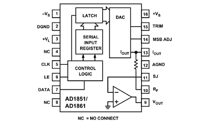
DescriptionThe AD1851/AD1861 is a monolithic PCM audio DAC. The AD1851 is a 16-bit device, while the AD1861 is an 18-bit device. Each device provides a voltage output amplifier, DAC, serial-to-parallel register and voltage reference. The digital portion of the AD1851/AD1861 is fabricated with CMOS logic elements that are provided by Analog Devices' 2 mm ABCMOS process. The analog portion of the AD1851/AD1861 is fabricated with bipolar and MOS devices as well as thin-film resistors.
This combination of circuit elements, as well as careful design and layout techniques, results in high performance audio playback. Laser-trimming of the linearity error affords low total harmonic distortion. An optional linearity trim pin is provided to allow residual differential linearity error at midscale to be eliminated. This feature is particularly valuable for low distortion
reproductions of low amplitude signals. Output glitch is also small, contributing to the overall high level of performance. The output amplifier achieves fast settling and high slew rates, providing a full ±3 V signal at load currents up to 8 mA. When used in current output mode, the AD1851/AD1861 provides a ±1 mA output signal. The output amplifier is short circuit
protected and can withstand indefinite shorts to ground.
The serial input interface consists of the clock, data and latch enable pins. The serial 2s complement data word is clocked into the DAC, MSB first, by the external clock. The latch enable
signal transfers the input word from the internal serial input register to the parallel DAC input register. The AD1851 input clock can support a 12.5 MHz data rate, while the AD1861 input
clock can support a 13.5 MHz data rate. This serial input port is compatible with second generation digital filter chips used in consumer audio products. These filters operate at oversampling
rates of 23, 43, 83 and 163 sampling frequencies.
The critical specifications of THD+N and signal-to-noise ratio are 100% tested for all devices.
The AD1851/AD1861 operates with ±5 V power supplies, making it suitable for home use markets. The digital supply, VL, can be separated from the analog supplies, VS and VS, for reduced digital crosstalk. Separate analog and digital ground pins are also provided. Power dissipation is 100 mW typical.
The AD1851/AD1861 is available in either a 16-pin plastic DIP or a 16-pin plastic SOIC package. Both packages incorporate the industry standard pinout found on the AD1856 and AD1860 PCM audio DACs. As a result, the AD1851/AD1861 is a drop-in replacement for designs where ±5 V supplies have been used with the AD1856/AD1860. Operation is guaranteed over the temperature range of 25°C to +70°C and over the voltage supply range of ±4.75 V to ±5.25 V.

 AD1851 Data Sheet


