Features: * Three chip set supporting full duplex serial transmission over twin optical fiber, one fiber with WDM.
* Configurable parallel microprocessor bus interface.
* Up to 16 independent synchronous data channels.
1 x OC1 (STS1) @ 51.840Mbps
1 x E3/T3
4 x E2, 7 x T2
16 x E1/T1
* Select between NRZ and pseudo-bipolar HDB3/AMI/B3ZS/B6ZS/B8ZS input data coding types.
* Incorporates 2 x 256kbps maintenance channels with optionof multi channel operation with a framing signal.
* Link budgets of 27dB with Laser + PIN on single mode fiber.
* Conforms to all jitter attenuation, jitter transfer and input jitter tolerance specification defined by AT&T, ITU-T and Bellcore recommendations.
* Bit Error Rate (BER) of < 10-10
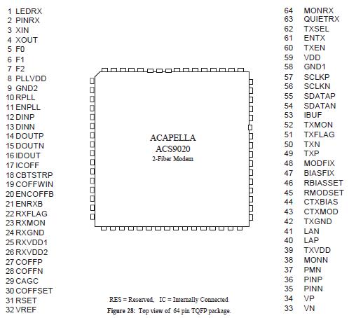
* ACS9020 available in 64 pin TQFP and ACS4110 available in 176 pin TQFP package.
Pinout Description
The ACS411CS is a complete controller, driver and receiver chipset supporting full-duplex synchronous transmission up to 51.840Mbps over single/twin optical fiber. The designer can share the available bandwidth over 1 to 16 main channels.
In addition to the main channels, the ACS411CS provides two independent maintenance channels with a data rate selectable up to 256kbps. On the electrical side the ACS411CS has a selectable interface for either NRZ or the pseudo bipolar data coding types HDB3/AMI/B3ZS/B6ZS/B8ZS.
The ACS411CS has a parallel microprocessor bus interface. This can be used for device set-up, diagnostics, control and status analysis. Additional flags for Tx data status, Rx data status and alarm indication for both near end and far end receive fail are accessible via the uP interface.Communicating modems automatically maintain synchronization with each.
The ACS411CS comprises a chip set of two/three (link budget dependent) highly integrated devices,the ACS9020 and ACS4110. The ACS9020 is an analogue device and the ACS4110 is predominately a digital device.
The ACS9020 contains the Laser/LED driver as well as the PIN receiver circuitry. Since the devices are transmitting and receiving continuously, for long haul applications two ACS9020 devices are required, one configured as the transmitter and the other configured as the receiver.
The ACS4110 comprises the logic necessary to time compress and decompress the data, plus clock recovery and all the logic associated with valid data transmission and reception and locking status. The ACS4110 also has a configurable parallel microprocessor bus interface for device configuration (control) and status analysis. The device setup is also possible via the far end (remote control) or directly via pins for the basic device setup.
For the purpose of this specification the chip-set ACS411CS will be referred to as the ACS411CS and the individual devices as the ACS9020 or ACS4110.
For low link budget applications (up to 10dB) two chips, the ACS9020 analogue IC (including laser driver and PIN receiver circuitry) and the ACS4110 are sufficient.
For applications requiring a higher link budget (up to 30dB) a three chip solution has to be used, where the laser driver and PIN receiver circuitry are separated.

 ACS411CS Data Sheet


