Features: VIN Range: 2.7V to 5.5VAdjustable± Dual Charge PumPositive Supply Output Up to +25VNegative Supply Output Down to -25VUp to 30mAOutput Current1.0MHz Switching Frequency<1.0AShutdown CurrenInternal Power MOSFETsInternally Controlled Soft StartFast Transient ResponseUltra-Thin Solution ...
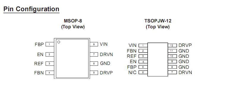
AAT3190: Features: VIN Range: 2.7V to 5.5VAdjustable± Dual Charge PumPositive Supply Output Up to +25VNegative Supply Output Down to -25VUp to 30mAOutput Current1.0MHz Switching Frequency<1.0AShutdown Cur...
SeekIC Buyer Protection PLUS - newly updated for 2013!
268 Transactions
All payment methods are secure and covered by SeekIC Buyer Protection PLUS.
The AAT3190 charge pump controller provides the regulated positive and negative voltage biases required by active matrix thin-film transistor (TFT) liquid-crystal displays (LCDs), CCD Sensors, and OLEDs. Two low-power charge pumps convert input supply voltages ranging from 2.7V to 5.5V into two independent output voltages. The dual low-power charge pumps independently regulate a positive (VPOS) and a negative (VNEG) output voltage. These outputs use external diode and capacitor multiplier stages (as many stages as required) to regulate output voltages up to *Plus-or-minus*25V. Built-in soft-start circuitry prevents excessive in-rush current during start up. A high switching frequency enables the use of small external capacitors. The device shutdown feature disconnects the load from VIN and reduces the quiescent current to less than 1.0A. The AAT3190 is available in an MSOP-8 or TSOPJW-12 package and is specified over a -40C to +85C operating temperature range.
The AAT3190 charge pump controller provides theregulated positive and negative voltage biases required by active matrix thin-film transistor (TFT) liquid-crystal displays (LCDs), charge-coupled device (CCD) sensors, and organic light emitting diodes (OLEDs). Two low-power charge pumps convert input supply voltages ranging from 2.7V to .5V into two independent output voltages. The dual low-power charge pumps independently regulate a positive (VPOS ) and negative (VNEG)out-put voltage. These outputs use external diode and capacitor multiplier stages (as many stages as required) to regulate output voltages up to ±25V uilt-in soft-start circuitry prevents excessive in- ush current during start-up. Ahigh switching fre- uency enables the use of small external capaci- ors. The device' shutdown feature disconnect he load from VIN and reduces quiescent current to ess than 1.0|A.