Features: • VIN Range: 2.7V to 5.5V
• 600mA Peak Output Current
• Tri-Mode 1X/1.5X/2X in Current Mode
• Voltage Mode Operation: 1.5X, 100mA
• Dual Regulated Current Sinks
• Current Match Between Current Sinks
• 32 Current Steps Set by AS2Cwire
• 1µF Input, Output, and Flying Capacitors
• <1.0µA of Shutdown
• Small Application Circuit
• No Inductors
• Automatic Soft Start
• 12-Pin TDFN 3x3 Package
• -40°C to +85°C Temperature RangeApplication• Camera Phones
• Digital Still Cameras (DSCs)
• PDAs and Notebook PCs
• Smart PhonesPinout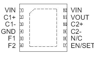 Specifications
- VIN Range: 2.7V to 5.5V
- 600mA Output Current
- Tri-Mode 1X/1.5X/2X in Current Mode
- Voltage Mode Operation: 1.5X, 100mA
- Dual Regulated Current Sinks
- Current Match Between Current Sinks
- 32 Current Steps Set by AS2Cwire
- 1F Input, Output, and Flying Capacitors
- <1.0A of Shutdown
- Small Application Circuit
- No Inductors
- Automatic Soft Start
- 12-Pin TDFN 3x3mm Package
- -40C to +85C Temperature Range
| Symbol |
Description |
Value |
Units |
| VIN |
Input Voltage |
-0.3 to 6.0 |
V |
| VEN |
EN to GND Voltage |
-0.3 to 6.0 |
V |
| VEN(MAX) |
Maximum EN to Input Voltage |
VIN + 0.3 |
V |
| IOUT |
Maximum DC Output Current (continuous) |
400 |
mA |
| TJ |
Operating Junction Temperature Range |
-40 to 150 |
°C |
| TS |
Storage Temperature Range |
-65 to 150 |
°C |
| TLEAD |
Maximum Soldering Temperature (at leads, 10 sec) |
300 |
°C |
Descriptionspan id="lblDescription">
The AAT3172 is a high output current, high efficiency, low noise, low profile charge pump DC/DC converter, ideal for multi-function LED photo-flash applications where solution cost, size, and efficiency are critical. The dual charge pump in the AAT3172 is capable of delivering 600mA output current. Two current-controlled paths are available for users of dual flash LEDs that prefer current matching. Each LED channel can be easily programmed in 32 steps with a single GPIO output through the AS2Cwire?(Advanced Simple Serial Control? interface. This allows smooth transitions and flexible adjustment of brightness in flash or other lighting modes. The tri-mode (1X/1.5X/2X) operation of the internal charge pump offers excellent power efficiency for both flash and movie modes. Combined with a low external parts count (two 1F flying capacitors and one small bypass capacitor at VIN and OUT), the AAT3172 is ideally suited for small, battery-powered applications. The AAT3172 has a thermal management system to protect the device in the event of a short-circuit condition at the output pin. Built-in soft-start circuitry prevents excessive inrush current during start-up. The shutdown feature disconnects the load from VIN and reduces quiescent current to less than 1.0A. The AAT3172 is available in the Pb-free, thermally-enhanced, 12-pin 3x3mm TDFN package.
The AAT3172 is a high output current, high efficiency, low noise, low profile charge pump DC/DC converter, ideal for multi-function LED photo-flash applications where solution cost, size, and efficiency are critical.
The dual charge pump in the AAT3172 is capable of delivering 600mA peak output current. Two current- controlled paths are available for users of dual flash LEDs that prefer current matching. Each LED channel can be easily programmed in 32 steps with a single GPIO output through the AS2Cwire™ (Advanced Simple Serial Control™) interface. This allows smooth transitions and flexible adjustment of brightness in flash or other lighting modes.
The tri-mode (1X/1.5X/2X) operation of the internal charge pump offers excellent power efficiency for both flash and movie modes. Combined with a low external parts count (two 1µF flying capacitors and one small bypass capacitor at VIN and OUT), the AAT3172 is ideally suited for small, battery-powered applications.
The AAT3172 has a thermal management system to protect the device in the event of a short-circuit condition at the output pin. Built-in soft-start circuitry prevents excessive inrush current during start-up. The shutdown feature disconnects the load from VIN and reduces quiescent current to less than 1.0µA.
The AAT3172 is available in the Pb-free, thermallyenhanced, 12-pin 3x3 TDFN package.

 AAT3172 Data Sheet