Series: -
Number of Outputs: 1
Mounting Type: Surface Mount
Evaluation Tools: -
Voltage - Load: -
Applications: PWM Motor Driver
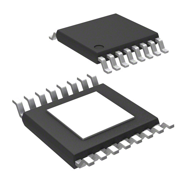
Package / Case: 16-TSSOP (0.173", 4.40mm Width) Exposed pad
Operating Temperature: -20°C ~ 85°C
Manufacturer: Allegro Microsystems Inc
Voltage - Supply: 8 V ~ 36 V
Supplier Device Package: 16-TSSOP-EP
Current - Output: ±2.8A
Packaging: Cut Tape (CT)
DescriptionThe A3949SLPTR-T is one member of the A3949 series.The A3949 is supplied in a choice of two power packages, a 16-pin plastic SOIC with a copper batwing tab (part number suffi x LB), and a low profi le (1.1mm) 16-pin TSSOP (suffi x LP) with exposed power tab. Both packages are available in a lead-free version (100% matte tin leadframe).
Features of the A3949SLPTR-T are:(1)single supply operation; (2)very small outline package; (3)low Rds(on) outputs; (4)sleep function; (5)internal UVLO; (6)crossover current protection; (7)thermal shutdown protection.PHASE and ENABLE input terminals are provided for use in controlling the speed and direction of a dc motor with externally applied PWM control signals. Internal synchronous rectifi cation control circuitry is provided to reduce power dissipation during PWM operation.Braking. The braking function is implemented by driving the device in slow decay mode via the MODE pin, and applying an enable chop command. Because it is possible to drive current in both directions through the DMOS switches, this confi guration effectively shorts out the motor-generated BEMF, as long as the enable chop mode is asserted on the ENABLE pin.
The absolute maximum ratings of the A3949SLPTR-T can be summarized as:(1)load supply voltage:36V;(2)operating junction temperature:150;(3)output current:±2.8 A;(4)sense voltage:0.5V;(5)logic input voltage:-0.3 to 7V;(6)storage temperature:-55 to 150.Control input SLEEP is used to minimize power consumption when the A3949 is not in use. This disables much of the internal circuitry, including the low-side gate supply and the charge pump. A logic low on this pin puts the device into Sleep mode. A logic high allows normal operation. After coming out of Sleep mode, the user should wait 1 ms before applying PWM signals, to allow the charge pump to stabilize.In the event of a fault due to excessive junction temperature, or low voltage on VCP or VREG, the outputs of the device are disabled until the fault condition is removed. At power-up, the UVLO circuit disables the drivers.
Parameters: | Technical/Catalog Information | A3949SLPTR-T |
| Vendor | Allegro Microsystems Inc (VA) |
| Category | Integrated Circuits (ICs) |
| Applications | PWM Motor Driver |
| Number of Outputs | 1 |
| Voltage - Supply | 8 V ~ 36 V |
| Voltage - Load | - |
| Current - Output | ±2.8A |
| Operating Temperature | -20°C ~ 85°C |
| Package / Case | 16-TSSOP |
| Packaging | Digi-Reel? |
| Lead Free Status | Lead Free |
| RoHS Status | RoHS Compliant |
| Other Names | A3949SLPTR T
A3949SLPTRT
620 1132 6 ND
62011326ND
620-1132-6
|

 A3949SLPTR-T Data Sheet


