Features: `Single power supply operation
- Full voltage range: 2.7 to 3.6 volt read and write perations for battery-powered applications
`Access times: 70/90 (max.)
`Current:
- 9 mA typical active read current
- 20 mA typical program/erase current
- 200 nA typical CMOS standby
- 200 nA Automatic Sleep Mode current
`Flexible sector architecture
- 16 Kbyte/ 8 KbyteX2/ 32 Kbyte/ 64 KbyteX15 sectors
- 8 Kword/ 4 KwordX2/ 16 Kword/ 32 KwordX15 sectors
- Any combination of sectors can be erased
- Supports full chip erase
- Sector protection: hardware method of protecting sectors to prevent any nadvertent program or erase operations within that sector
`Extended operating temperature range: -40 ~ +85 for - series; -25 ~ +85 for I series
`Unlock Bypass Program Command
- Reduces overall programming time when issuing multiple rogram command sequence
`Top or bottom boot block configurations available
`Embedded Algorithms
- Embedded Erase algorithm will automatically erase the ntire chip or any combination of designated sectors and
verify the erased sectors
- Embedded Program algorithm automatically writes and erifies data at specified addresses
`Typical 100,000 program/erase cycles per sector
`20-year data retention at 125
- Reliable operation for the life of the system
`Compatible with JEDEC-standards
- Pinout and software compatible with single-power-supply lash memory standard
- Superior inadvertent write protection
`Data Polling and toggle bits
- Provides a software method of detecting completion of rogram or erase operations
`Ready / BUSY pin (RY / BY)
- Provides a hardware method of detecting completion of rogram or erase operations (not available on 44-pin OP)
`Erase Suspend/Erase Resume
- Suspends a sector erase operation to read data from, or rogram data to, a non-erasing sector, then resumes the
erase operation
`Hardware reset pin (RESET )
- Hardware method to reset the device to reading array data
`Package options
- 44-pin SOP or 48-pin TSOP (I) or 48-ball TFBGA
Pinout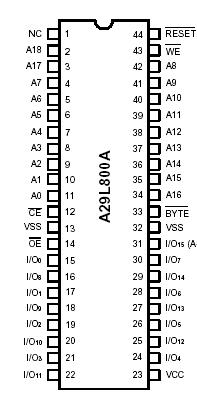 Specifications
Storage Temperature Plastic Packages. . . . . . . . .. . . . . . . . . .-65 to + 150
Ambient Temperature with Power Applied. . . . . . . . .. . . . . . . -55 to + 125
Voltage with Respect to Ground VCC (Note 1) . . . . . . . . . . . . . .-0.5V to +4.0V
A9,OE &RESET (Note 2) . . . . . . . . . . . . . . . .. . . . . . . . . . . . . . . .-0.5 to +12.5V
All other pins (Note 1) . . . . . . . . . .. . . .. . . . . . . . . . . . .. .-0.5V to VCC + 0.5V
Output Short Circuit Current (Note 3) . . . . . . . . . . . . . . . . . . .. . . . . . . .200mA
1. Minimum DC voltage on input or I/O pins is -0.5V. During voltage transitions, input or I/O pins may undershoot VSS to -2.0V for periods of up to 20ns. Maximum DC voltage on input and I/O pins is VCC +0.5V. During voltage ansitions,
input or I/O pins may overshoot to VCC +2.0V for periods up to 20ns.
2. Minimum DC input voltage on A9,OE and RESET is - 0.5V. During voltage transitions, A9,OE and RESET may overshoot VSS to -2.0V for periods of up to 20ns. Maximum DC input voltage on A9 is +12.5V which may overshoot to
14.0V for periods up to 20ns.
3. No more than one output is shorted at a time. Duration of the short circuit should not be greater than one second.
DescriptionThe A29L800A is an 8Mbit, 3.0 volt-only Flash memory rganized as 1,048,576 bytes of 8 bits or 524,288 words of 16
bits each. The 8 bits of data appear on I/O0 - I/O7; the 16 bits of ata appear on I/O0~I/O15. The A29L800A is offered in 48-ball FBGA, 44-pin SOP and 48-Pin TSOP packages. This device s designed to be programmed in-system with the standard ystem 3.0 volt VCC supply. Additional 12.0 volt VPP is not equired for in-system write or erase operations. However, the 29L800A can also be programmed in standard EPROM rogrammers.
The A29L800A has the first toggle bit, I/O6, which indicates hether an Embedded Program or Erase is in progress, or it is n the Erase Suspend. Besides the I/O6 toggle bit, the 29L800A has a second toggle bit, I/O2, to indicate whether
the addressed sector is being selected for erase. The 29L800A also offers the ability to program in the Erase uspend mode. The standard A29L800A offers access times f 70 and 90ns, allowing high-speed microprocessors to perate without wait states. To eliminate bus contention the evice has separate chip enable (CE ), write enable ( WE ) nd output enable (OE ) controls.
The device A29L800A requires only a single 3.0 volt power supply for oth read and write functions. Internally generated and
regulated voltages are provided for the program and erase perations.
The A29L800A is entirely software command set compatible ith the JEDEC single-power-supply Flash standard. ommands are written to the command register using tandard microprocessor write timings. Register contents serve
as input to an internal state-machine that controls the erase nd programming circuitry. Write cycles also internally latch ddresses and data needed for the programming and erase perations. Reading data out of the device is similar to reading rom other Flash or EPROM devices.
Device programming occurs by writing the proper program ommand sequence. This initiates the Embedded Program
algorithm - an internal algorithm that automatically times the rogram pulse widths and verifies proper program argin.
Device A29L800A erasure occurs by executing the proper erase ommand sequence. This initiates the Embedded Erase lgorithm - an internal algorithm that automatically reprograms the array (if it is not already programmed) before xecuting the erase operation. During erase, the device utomatically times the erase pulse widths and verifies proper rase margin. The Unlock Bypass mode facilitates faster rogramming times by requiring only two write cycles to rogram data instead of four.
The host system can detect whether a program or erase peration is complete by observing the RY / BY pin, or by eading the I/O7 (Data Polling) and I/O6 (toggle) status bits.

 A29L800A Series Data Sheet


