Features: Simultaneous Read/Write operations
- Data can be continuously read from one bank while
executing erase/program functions in other bank
- Zero latency between read and write operations
Multiple bank architectures
- Three devices available with different bank sizes (refer to Table 2)
Package options
- 48-ball TFBGA
- 48-pin TSOP
Top or bottom boot block
Manufactured on 0.18 µm process technology
- Compatible with AMD AM29DL32xD device
Compatible with JEDEC standards
- Pinout and software compatible with single-power-supply flash standard
PERFORMANCE CHARACTERISTICS
High performance
- Access time as fast as 70ns
- Program time: 7µs/word typical utilizing Accelerate function
Ultra low power consumption (typical values)
- 2mA active read current at 1MHz
- 10mA active read current at 5MHz
- 200nA in standby or automatic sleep mode
Minimum 1 million write cycles guaranteed per sector
20 Year data retention at 125°C
- Reliable operation for the life of the system
SOFTWARE FEATURES
Supports Common Flash Memory Interface (CFI)
Erase Suspend/Erase Resume
- Suspends erase operations to allow programming in
Data Polling and Toggle Bits
- Provides a software method of detecting the status of program or erase cycles
Unlock Bypass Program command
- Reduces overall programming time when issuing multiple program command sequences
HARDWARE FEATURES
Any combination of sectors can be erased
Ready/Busy output (RY/By)
- Hardware method for detecting program or erase cycle completion
Hardware reset pin (RESET)
- Hardware method of resetting the internal state machine to reading array data
WP /ACC input pin
- Write protect ( WP ) function allows protection of two outermost boot sectors, regardless of sector protect status
- Acceleration (ACC) function accelerates program timing
Sector protection
- Hardware method of locking a sector, either in-system or using programming equipment, to prevent any program or erase operation within that sector
- Temporary Sector Unprotect allows changing data in protected sectors in-system same bank
Software temporary sector/sector block unprotect command
Software sector protect/unprotect command
Pinout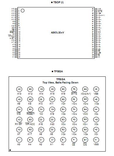 SpecificationsStorage Temperature Plastic Packages. . . . -65°C to + 150°C
Ambient Temperature with Power Applied. . -65°C to + 125°C
Voltage with Respect to Ground
VCC (Note 1) . . . . . . . . . . . . . . . . . . . . . . . . . . . -0.5V to +4.0V
A9, OE & RESET (Note 2) . . . . . . . . . . . . . . . . -0.5V to +12.5V
WP /ACC . . . . . . . . . . . . . . . . . . . . . . . . . . . . . . -0.5V to +10.5V
All other pins (Note 1) . . . . . . . . . .. . . . . . . -0.5V to VCC + 0.5V
Output Short Circuit Current (Note 3) . . . . . . . . . . . . . . .200mA DescriptionThe A29DL32x family consists of 32 megabit, 3.0 volt-only flash memory devices, organized as 2,097,152 words of 16 bits each or4,194,304 bytes of 8 bits each. Word mode data appears on I/O0I/O15; byte mode data appears on I/O0I/O7. The device is designed to be programmed in-system with the standard 3.0 volt VCC supply, and can also be programmed in standard EPROM programmers.
The device A29DL32x is available with an access time of 70, 80, 90, or 120 ns. The devices are offered in 48-pin TSOP and 48-ball Fine-pitch TFBGA. Standard control pins-chip enable (CE ), write enable ( WE ), and output enable ( OE )-control normal read and write operations, and avoid bus contention issues. The device requires only a single 3.0 volt power supply for both read and write functions. Internally generated and regulated voltages are provided for the program and erase operations.

 A29DL32x Data Sheet


