9DB102BFLF

Clock Buffer 2 OUTPUT PCIE GEN2 BUFFER

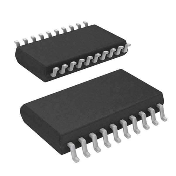
product image

9DB102BFLF Picture
SeekIC No. : 00312542 Detail

9DB102BFLF: Clock Buffer 2 OUTPUT PCIE GEN2 BUFFER

floor Price/Ceiling Price

US $ 1.41~2.14 / Piece | Get Latest Price
Part Number:
9DB102BFLF
Mfg:
IDT
Supply Ability:
5000

Price Break

  • Qty
  • 0~1
  • 1~10
  • 10~100
  • 100~250
  • Unit Price
  • $2.14
  • $1.72
  • $1.57
  • $1.41
  • Processing time
  • 15 Days
  • 15 Days
  • 15 Days
  • 15 Days
View more price & deliveries
Total Cost: $ 0.00

SeekIC Buyer Protection PLUS - newly updated for 2013!

  • Escrow Protection.
  • Guaranteed refunds.
  • Secure payments.
  • Learn more >>

Month Sales

268 Transactions

Rating

evaluate  (4.8 stars)

Upload time: 2024/10/17

Payment Methods

All payment methods are secure and covered by SeekIC Buyer Protection PLUS.
Notice: When you place an order, your payment is made to SeekIC and not to your seller. SeekIC only pays the seller after confirming you have received your order. We will also never share your payment details with your seller.
Product Details

Quick Details

Number of Outputs : 2 Max Input Freq : 100 MHz
Supply Voltage - Max : 3.465 V Supply Voltage - Min : 3.135 V
Maximum Operating Temperature : + 70 C Minimum Operating Temperature : 0 C
Package / Case : QSOP-20    

Description

Propagation Delay (Max) :
Maximum Power Dissipation :
Packaging :
Number of Outputs : 2
Max Input Freq : 100 MHz
Maximum Operating Temperature : + 70 C
Minimum Operating Temperature : 0 C
Supply Voltage - Max : 3.465 V
Supply Voltage - Min : 3.135 V
Package / Case : QSOP-20


Specifications

Temperature C Voltage 3.3 V Package QSOP 20 Speed NA Output Style Core Supply Voltage (VDD) No. of Outputs Min. Output Frequency Min. Input Frequency Output Supply Voltage (VDDO) No. of Inputs Input Style Max. Output Frequency Max. Input Frequency Temp. Grade Multiplication/Divide Value


Description

PCI EXPRESS BUFFER
1-to-2 Zero-delay or fanout buffer for PCI Express.The ICS9DB102 zero-delay buffer supports PCI Express clocking requirements. The ICS9DB102 is driven by a differential SRC output pair from an ICS CK409/CK410-compliant main clock generator such as the ICS952601 or ICS954101. It attenuates jitter on the input clock and has a selectable PLL Band Width to maximize performance in systems with or without Spread- Spectrum clocking.


Customers Who Bought This Item Also Bought

Margin,quality,low-cost products with low minimum orders. Secure your online payments with SeekIC Buyer Protection.
Soldering, Desoldering, Rework Products
Programmers, Development Systems
Cables, Wires - Management
Circuit Protection
Semiconductor Modules
Hardware, Fasteners, Accessories
View more