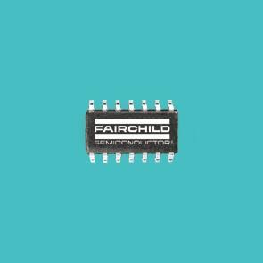
Features: 5V tolerant inputs and outputs2.3V − 3.6V VCC specifications provided7.0 ns tPD max (VCC = 3.3V), 10 µA ICC maxPower down high impedance inputs and outputsSupports live insertion/withdrawal (Note 1)±24 mA output drive (VCC = 3.0V)Implements patented noise/EMI reduction circui...
74LCX652: Features: 5V tolerant inputs and outputs2.3V − 3.6V VCC specifications provided7.0 ns tPD max (VCC = 3.3V), 10 µA ICC maxPower down high impedance inputs and outputsSupports live inserti...
SeekIC Buyer Protection PLUS - newly updated for 2013!
268 Transactions
All payment methods are secure and covered by SeekIC Buyer Protection PLUS.
US $.23 - .39 / Piece
Gates (AND / NAND / OR / NOR) Quad 2-Input NAND Gate with 5V Tol Inp
Symbol | Parameter | Value | Conditions | Units |
VCC | Supply Voltage | −0.5 to +7.0 | V | |
VI | DC Input Voltage | −0.5 to +7.0 | V | |
VO | DC Output Voltage | −0.5 to +7.0 −0.5 to VCC + 0.5 |
Output in 3-STATE Output in HIGH or LOW State (Note 4) |
V |
IIK | DC Input Diode Current | −50 | VI < GND | mA |
IOK | DC Output Diode Current | −50 +50 |
VO < GND VO > VCC |
mA |
IO | DC Output Source/Sink Current | ±50 | mA | |
ICC | DC Supply Current per Supply Pin | ±100 | mA | |
IGND | DC Ground Current per Ground Pin | ±100 | mA | |
TSTG | Storage Temperature | −65 to +150 | °C |
The 74LCX652 consists of bus transceiver circuits with Dtype flip-flops, and control circuitry arranged for multiplexed transmission of data directly from the input bus or from internal registers. Data on the A or B bus will be clocked into the registers as the appropriate clock pin goes to the HIGH logic level. Output Enable pins (OEAB, OEBA) are provided to control the transceiver function.
The 74LCX652 is designed for low voltage (2.5V or 3.3V) VCC applications with capability of interfacing to a 5V signal environment.
The 74LCX652 is fabricated with an advanced CMOS technology to achieve high speed operation while maintaining CMOS low power dissipation.