Polarity
: Non-Inverting
Maximum Operating Temperature
: + 85 C
Mounting Style
: SMD/SMT
Supply Voltage - Min
: 2 V
Supply Voltage - Max
: 3.6 V
Number of Input Lines
: 4
Number of Output Lines
: 4
Packaging
: Tube
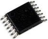
Package / Case
: SOIC-14
Features: ` 5V tolerant inputs and outputs
` 2.3V3.6V VCC specifications provided
` 6.0 ns tPD max (VCC = 3.3V), 10 A ICC max
` Power down high impedance inputs and outputs
` Supports live insertion/withdrawal (Note 1)
` ±24 mA output drive (VCC = 3.0V)
` Implements patented noise/EMI reduction circuitry
` Latch-up performance exceeds 500 mA
` ESD performance:
Human body model > 2000V
Machine model > 100VPinout
 Specifications
| Symbol |
Parameter |
Value |
Conditions |
Units |
| VCC |
Supply Voltage |
-0.5 to +7.0 |
|
V |
| VI |
DC Input Voltage |
-0.5 to +7.0 |
|
V |
| VO |
DC Output Voltage |
-0.5 to +7.0
-0.5 to VCC + 0.5
|
-Output in 3-STATE
Output in HIGH or LOW State (Note4)
|
V |
| LIK |
DC Input Diode Current |
-50 |
VI < GND |
mA |
| LOK |
DC Output Diode Current |
-50
+50 |
VO < GND
VO > VCC |
mA |
| LO |
DC Output Source/Sink Current |
±50 |
|
mA |
| LCC |
DC Supply Current per Supply Pin |
±100 |
|
mA |
| LANG |
DC Ground Current per Ground Pin |
±100 |
|
mA |
| TSTG |
Storage Temperature |
-65 to +150 |
|
°C |
DescriptionThe 74LCX125M contains four independent non-inverting buffers with 3-STATE outputs. The inputs tolerate voltages up to 7V allowing the interface of 5V systems to 3V systems. The 74LCX125 is fabricated with an advanced CMOS technology to achieve high speed operation while maintaining CMOS low power dissipation.
The 74LCX125M is a type of low voltage quad with 5V tolerant inputs and outputs, which contains four independent non-inverting buffers with 3-STATE outputs. The inputs tolerate voltages can reach 7V allowing the interface of 5V systems to 3V systems.The 74LCX125 is fabricated with an advanced CMOS technology to achieve high speed ope-ration when maintaining CMOS low power dissipation.
The 74LCX125M has some unique features shown below:(1)5V tolerant inputs and outputs;(2)2.3V-3.6V VCC specific- ations provided;(3)6.0 ns tPD max (VCC -3.3V), 10 uA ICC max;(4)power down high impedance inputs and outputs;(5)±24 mA output drive (VCC -3.0V);(6)implements patented noise/EMI reduction circuitry;(7)latch-up performance exceeds JEDEC 78 conditions;(8)ESD performance are human body model is greater than 2000V and machine model is greater than 100V;(9)leadless Pb-Free DQFN package;etc.
Some absolute maximum ratings of the 74LCX125M (The Absolute Maximum Ratings are those values beyond which the safety of the device cannot be guaranteed. The device should not be operated at these limits)have been concluded as following:(1):supply voltage is -0.5 V to +7.0 V;(2):DC input voltage is -0.5 V to+7.0 V;(3):DC output voltage is -0.5 V to VCC +0.5 V when output in high or low state, and DC output voltage is -0.5V to +7V when output in 3-state ;(4):DC input diode current is -50 mA when VI is less than GND;(5):DC output diode current is -50 mA when VO is less than GND, or DC output diode current is +50 mA when VO is is greater than VCC;(6):DC output source/sink current is ±50 mA;(7):DC supply current per supply Pin is ±100 mA;(8):DC ground current per ground pin is ±100 mA;(9):storage temperature is -65 to +150.
All in all , this is a simple decription of the 74LCX125M, if you want to know more about it, please pay more attention to our web!
Parameters: | Technical/Catalog Information | 74LCX125M |
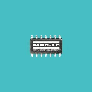
| Vendor | Fairchild Optoelectronics Group |
| Category | Integrated Circuits (ICs) |
| Logic Type | Line Driver, Non-Inverting |
| Package / Case | 14-SOIC |
| Packaging | Tube |
| Mounting Type | Surface Mount |
| Number of Bits per Element | 1 |
| Number of Elements | 4 - Quad |
| Operating Temperature | -40°C ~ 85°C |
| Voltage - Supply | 2 V ~ 3.6 V |
| Current - Output High, Low | 24mA, 24mA |
| Lead Free Status | Lead Free |
| RoHS Status | RoHS Compliant |
| Other Names | 74LCX125M
74LCX125M
|
 74LCX125M Data Sheet