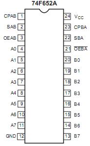
Features: *Combines 74F245 and two 74F374 type functions in one chip*High impedance base inputs for reduced loading (70µA in high and low states)*Independent registers for A and B buses*Multiplexed real-time and stored data*Choice of non-inverting and inverting data paths*3-State outputs*Ind...
74F652A: Features: *Combines 74F245 and two 74F374 type functions in one chip*High impedance base inputs for reduced loading (70µA in high and low states)*Independent registers for A and B buses*Multip...
SeekIC Buyer Protection PLUS - newly updated for 2013!
268 Transactions
All payment methods are secure and covered by SeekIC Buyer Protection PLUS.
SYMBOL | PARAMETER | RATING | UNIT | |
VCC | Supply voltage | 0.5 to +7.0 | V | |
VIN | Input voltage | 0.5 to +7.0 | V | |
IIN | Input current | 30 to +5 | mA | |
VOUT | Voltage applied to output in high output state | 0.5 to VCC | V | |
IOUT | Current applied to output in low output state | Commercial range | 72 | mA |
Industrial range | 0 to +70 | °C | ||
Tamb | Operating free air temperature range | 40 to +85 | °C | |
Tstg | Storage temperature range | 65 to +150 | °C |
The 74F652A transceivers/registers consist of bus transceiver circuits with 3State outputs, Dtype flipflops, and control circuitry arranged for multiplexed transmission of data directly from the input bus or the internal registers. Data on the A or B bus will be clocked into the registers as the appropriate clock pin goes high. Output enable (OEAB, OEBA) and select (SAB, SBA) pins of the 74F652A are provided for bus management.