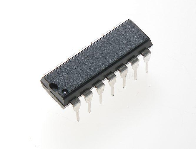
Features: · Guaranteed 30 MHz data rate
· Six selectable polynomials
· Other polynomials available
· Separate preset and clear controls
· Expandable
· Automatic right justification
· Error output open collector
· Typical applications:Floppy and other disk storage systems Digital cassette and cartridge systems Data communication systems
ApplicationIn addition to polynomial selection there are four other capabilities provided for in the 'F402 ROM. The first is set or clear selectability. The sixteen internal registers have the capability to be either set or cleared when P is brought LOW. This set or clear capability is done in four groups of 4 (see Table II, P0±P3). The second ROM capability (C0) is in determining the polarity of the check word. As is the case with the Ethernet polynomial the check word can be inverted when it is appended to the data stream or as is the case with the other polynomials, the residue is appended with no inversion. Thirdly, the ROM contains a bit (C1) which is used to select the RFB input instead of the SEI input to be fed into the LSB. This is used when the polynomial selected is actually a residue (least significant) stored in the ROM which indicates whether the selected location is a polynomial or a residue. If the latter, then it inhibits the RFB input.
As mentioned previously, upon a successful data transmission, the CRC register has a zero residue. There is an exception to this, however, with respect to the Ethernet polynomial. This polynomial, upon a successful data transmission, has a non-zero residue in the CRC register (C7 04 DD 7B)16. In order to provide a no-error indication, two ROM locations have been preloaded with the residue so that by selecting these locations and clocking the device one additional time, after the last check bit has been entered, will result in zeroing the CRC register. In this manner a no-error indication is achieved.
With the present mix of polynomials, the largest is 56th order requiring four devices while the smallest is 16th order requiring just one device. In order to accommodate multiplexing between high order polynomials (X 16th order) and lower order polynomials, a location of all zeros is provided.This allows the user to choose a lower order polynomial even if the system is configured for a higher order one.
The 'F402 expandable CRC generator checker contains 6 popular CRC polynomials, 2-16th Order, 2-32nd Order, 1- 48th Order and 1-56th Order. The application diagram shows the 'F402 connected for a 56th Order polynomial.Also shown are the input patterns for other polynomials.When the 'F402 is used with a gated clock, disabling the clock in a HIGH state will ensure no erroneous clocking occurs when the clock is re-enabled. Preset and Master Reset are asynchronous inputs presetting the register to S or clearing to 1s respectively (note Ethernet residue and 56th Order select code 8, LSB, are exceptions to this).
To generate a CRC, the pattern for the selected polynomial is applied to the S inputs, the register is preset or cleared as required, clock is enabled, CWG is set HIGH, data is applied to D input, output data is on D/CW. When the last data bit has been entered, CWG is set LOW and the register is clocked for n bits (where n is the order of the polynomial). The clock may now be stopped if desired (holding CWG LOW and clocking the register will output zeros from D/CW after the residue has been shifted out).
To check a CRC, the pattern for the selected polynomial is applied to the S inputs, the register is preset or cleared as required, clock is enabled, CWG is set HIGH, the data stream including the CRC is applied to D input. When the last bit of the CRC has been entered, the ER output is checked: HIGHeerror free data, LOWecorrupt data. The clock may now be stopped if desired.
To implement polynomials of lower order than 56th, select the number of packages required for the order of polynomial and apply the pattern for the selected polynomial to the S inputs (0000 on S inputs disables the package from the feedback chain).
Pinout Specifications
If Military/Aerospace specified devices are required,please contact the National Semiconductor Sales Office/Distributors for availability and specifications.
Storage Temperature .......................-65 to +150
Ambient Temperature under Bias..... -55 to +125
Junction Temperature under Bias..... -55 to +175
Plastic.............................................. -55 to +150
VCC Pin Potential to Ground Pin ........-0.5V to +7.0V
Input Voltage (Note 2) .....................-0.5V to +7.0V
Input Current (Note 2) ...............-30 mA to +5.0 mA
Voltage Applied to Output in HIGH State (with VCC = 0V)
Standard Output................................. b0.5V to VCC
TRI-STATE Output .........................-0.5V to +5.5V
Current Applied to Output in LOW State (Max)....... twice the rated IOL (mA)
Note 1: Absolute maximum ratings are values beyond which the device may be damaged or have its useful life impaired. Functional operation under these conditions is not implied.
Note 2: Either voltage limit or current limit is sufficient to protect inputs.
DescriptionThe 74F402 expandable Serial Data Polynomial generator/checker is an expandable version of the 'F401. It provides an advanced tool for the implementation of the most widely used error detection scheme in serial digital handling systems.
A 4-bit control input selects one-of-six generator polynomials.The list of polynomials includes CRC-16, CRCCCITT and EthernetÉ, as well as three other standard polynomials (56th order, 48th order, 32nd order). Individual clear and preset inputs are provided for floppy disk and other applications. The Error output indicates whether or not a transmission error has occurred. The CWG Control input inhibits feedback during check word transmission. The 74F402 is compatible with FASTÉ devices and with all TTL families.

 74F402 Data Sheet


