Features: • 4-bit parallel load shift register• Independent 3-State buffer outputs, Q0Q3• Separate Qs output for serial expansion• Asynchronous Master ResetPinoutSpecifications SYMBOL PARAMETER RATING UNIT VCC Supply voltage 0.5 to +7.0 V VIN I...
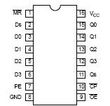
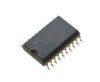
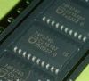
74F395: Features: • 4-bit parallel load shift register• Independent 3-State buffer outputs, Q0Q3• Separate Qs output for serial expansion• Asynchronous Master ResetPinoutSpecificatio...
SeekIC Buyer Protection PLUS - newly updated for 2013!
268 Transactions
All payment methods are secure and covered by SeekIC Buyer Protection PLUS.
SYMBOL |
PARAMETER |
RATING |
UNIT | |
VCC | Supply voltage |
0.5 to +7.0 |
V | |
VIN | Input voltage |
0.5 to +7.0 |
V | |
IIN | Input current |
30 to +5 |
mA | |
VOUT | Voltage applied to output in high output state |
0.5 to+5.5 |
V | |
IOUT | Current applied to output in low output state | Qs |
40 |
mA |
Q0Q3 |
48 |
mA | ||
Tamb | Operating free air temperature range |
0 to +70 |
°C | |
Tstg | Storage temperature range |
65 to +150 |
°C |
The 74F395 is a 4-bit Shift Register with serial and parallel synchronous operating modes and 3-State buffer outputs. The shifting and loading operations are controlled by the state of the Parallel Enable (PE) input. When PE is High, data is loaded from the Parallel Data inputs (D0D3) into the register synchronous with the High-to-Low transition of the Clock input (CP). When PE is Low, the data at the Serial Data input (Ds) is loaded into the Q0 flip-flop, and the data in the register is shifted one bit to the right in the direction (Q0Q1Q2Q3) synchronous with the negative clock transition. The PE and Data inputs are fully edge-triggered and must be stable one setup prior to the High-to-Low transition of the clock.
The Master Reset (MR) of the 74F395 is an asynchronous active-Low input. When Low, the MR overrides the clock and all other inputs and clears the register.
The 3-state output buffers of the 74F395 are designed to drive heavily loaded 3-State buses, or large capacitive loads.
The active-Low Output Enable (OE) of the 74F395 controls all four 3-State buffers independent of the register operation. The data in the register appears at the outputs when OE is Low. The outputs are in High impedance "OFF" state, which means they will neither drive nor load the bus when OE is High. The output of the 74F395 from the last stage is brought out separately. This output (Qs) is tied to the Serial Data input (Ds) of the next register for serial expansion applications. The Qs output is not affected by the 3-State buffer operation.