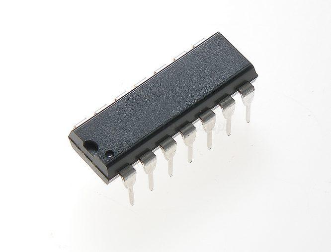
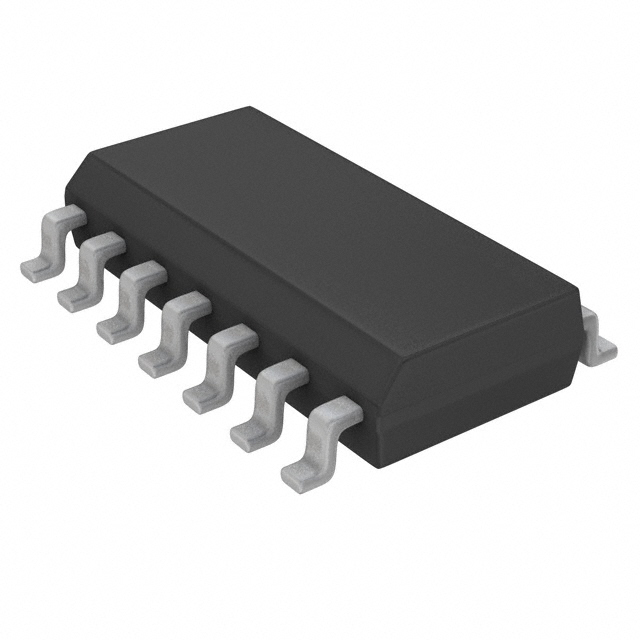
Features: • High speed performance• Replaces 74F219• Address access time: 8ns max vs 28ns for 74F219• Power dissipation: 4.3mW/bit typ• Schottky clamp TTL• One chip enable• NonInverting outputs (for inverting outputs see 74F189A)• 3state outputs̶...
74F219A: Features: • High speed performance• Replaces 74F219• Address access time: 8ns max vs 28ns for 74F219• Power dissipation: 4.3mW/bit typ• Schottky clamp TTL• One ch...
SeekIC Buyer Protection PLUS - newly updated for 2013!
268 Transactions
All payment methods are secure and covered by SeekIC Buyer Protection PLUS.
SYMBOL | PARAMETER | RATING | UNIT |
VCC | Supply voltage | 0.5 to +7.0 | V |
VIN | Input voltage | 0.5 to +7.0 | V |
IIN | Input current | 30 to +5 | mA |
VOUT | Voltage applied to output in High output state | 0.5 to VCC | V |
IOUT | Current applied to output in Low output state | 48 | mA |
Tamb | Operating free-air temperature range | 0 to +70 | °C |
Tstg | Storage temperature range | 65 to +150 | °C |
The 74F219A is a high speed, 64bit RAM organized as a 16word by 4bit array. Address inputs are buffered to minimize loading and are fully decoded on chip. The outputs are in high impedance state whenever the chip enable (CE) is high. The outputs are active only in the READ mode (WE = high) and the output data of the 74F219A is the complement of the stored data.