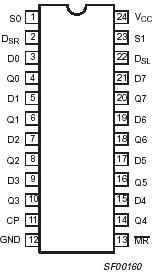
Features: • Buffered clock and control inputs
• Shift right, shift left, and parallel load capability
• Asynchronous Master ResetPinout Specifications
|
SYMBOL |
PARAMETER |
RATING |
UNIT |
|
VCC |
Supply voltage |
0.5 to +7.0 |
V |
|
VIN |
Input voltage |
0.5 to +7.0 |
V |
|
IIN |
Input current |
30 to +5 |
mA |
|
VOUT |
Voltage applied to output in high output state |
0.5 to VCC |
V |
|
IOUT |
Current applied to output in low output state |
40 |
mA |
|
Tamb |
Operating free air temperature range |
0 to +70 |
°C |
|
Tstg |
Storage temperature range |
65 to +150 |
°C |
DescriptionThe 74F198 Bidirectional Universal Shift Register is designed to incorporate virtually all of the features a system designer may want in a shift register. This circuit features parallel inputs and outputs, shift right and shift left serial inputs, operating mode select inputs, and direct overriding master reset input. The register has four distinct modes of operation:
Parallel (broadside) load
Shift right (in the direction Q0 toward Q7)
Shift left (in the direction Q7 toward Q0)
Inhibit clock (do nothing).
Synchronous parallel loading of the 74F198 is accomplished by applying the 8 bits of data and taking both mode control inputs, S0 and S1,High.The data is loaded into the associated flip-flop and appears at the outputs after the positive transition of the clock inputs. During loading, serial data flow is inhibited.
Shift right is accomplished synchronously, with the rising edge of the clock pulse when S0 is High and S1 is Low. Serial data for this mode is entered at the right data input (D
SR). When S0 is Low and S1 is High, data shifts left synchronously and new data is entered at the shift-left serial input (D
SL).
Clocking of the flip-flops of the 74F198 is inhibited when both mode control inputs are Low.

 74F198 Data Sheet


