74AUP2G00

Features: ` Wide supply voltage range from 0.8 V to 3.6 V` High noise immunity`Complies with JEDEC standards: JESD8-12 (0.8 V to 1.3 V) JESD8-11 (0.9 V to 1.65 V) JESD8-7 (1.2 V to 1.95 V) JESD8-5 (1.8 V to 2.7 V) JESD8-B (2.7 V to 3.6 V)` ESD protection: HBM JESD22-A114-D Class 3A exceeds 4...

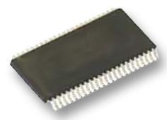
product image

74AUP2G00 Picture
SeekIC No. : 004249548 Detail

74AUP2G00: Features: ` Wide supply voltage range from 0.8 V to 3.6 V` High noise immunity`Complies with JEDEC standards: JESD8-12 (0.8 V to 1.3 V) JESD8-11 (0.9 V to 1.65 V) JESD8-7 (1.2 V to 1.95 V) JESD8...

floor Price/Ceiling Price

Part Number:
74AUP2G00
Supply Ability:
5000

Price Break

  • Qty
  • 1~5000
  • Unit Price
  • Negotiable
  • Processing time
  • 15 Days
Total Cost: $ 0.00

SeekIC Buyer Protection PLUS - newly updated for 2013!

  • Escrow Protection.
  • Guaranteed refunds.
  • Secure payments.
  • Learn more >>

Month Sales

268 Transactions

Rating

evaluate  (4.8 stars)

Upload time: 2024/12/21

Payment Methods

All payment methods are secure and covered by SeekIC Buyer Protection PLUS.

Notice: When you place an order, your payment is made to SeekIC and not to your seller. SeekIC only pays the seller after confirming you have received your order. We will also never share your payment details with your seller.
Product Details

Description


Features:

` Wide supply voltage range from 0.8 V to 3.6 V
` High noise immunity
`Complies with JEDEC standards:
   JESD8-12 (0.8 V to 1.3 V)
   JESD8-11 (0.9 V to 1.65 V)
   JESD8-7 (1.2 V to 1.95 V)
   JESD8-5 (1.8 V to 2.7 V)
   JESD8-B (2.7 V to 3.6 V)
` ESD protection:
   HBM JESD22-A114-D Class 3A exceeds 4000 V
   MM JESD22-A115-A exceeds 200 V
   CDM JESD22-C101-C exceeds 1000 V
` Low static power consumption; ICC = 0.9 mA (maximum)
`Latch-up performance exceeds 100 mA per JESD 78 Class II
` Inputs accept voltages up to 3.6 V
` Low noise overshoot and undershoot < 10 % of VCC
` IOFF circuitry provides partial Power-down mode operation
` Multiple package options
`Specified from -40to +85and -40 to +125


Pinout

  Connection Diagram


Specifications

Symbol
Parameter
Conditions
Min
Max
Unit
VCC
supply voltage  
-0.5
+4.6
V
IIK
input clamping current VI < 0 V
-
-50
mA
VI
input voltage

[1]

-0.5
+4.6
V
IOK
output clamping current VO < 0 V
-
-50
mA
VO
output voltage Active mode and Power-down mode      [1]
-0.5
+4.6
V
IO
output current VO = 0 V to VCC
-
±20
mA
ICC
supply current  
-
+50
mA
IGND
ground current  
-
-50
mA
Tstg
storage temperature  
-65
+150
Ptot
total power dissipation Tamb = -40 to +125                       [2]
-
250
mW
[1] The minimum input and output voltage ratings may be exceeded if the input and output current ratings
      are observed.
[2] For VSSOP8 packages: above 110 the value of Ptot derates linearly with 8.0 mW/K. For XSON8 and
     XQFN8 packages: above 45 the value of Ptot derates linearly with 2.4 mW/K.


Description

The 74AUP2G00 is a high-performance, low-power, low-voltage, Si-gate CMOS device, superior to most advanced CMOS compatible TTL families.

Schmitt-trigger action at all inputs makes the circuit tolerant to slower input rise and fall times across the entire VCC range from 0.8 V to 3.6 V.

The 74AUP2G00 ensures a very low static and dynamic power consumption across the entire VCC range from 0.8 V to 3.6 V.

The 74AUP2G00 is fully specified for partial Power-down applications using IOFF.

The IOFF circuitry of the 74AUP2G00 disables the output, preventing the damaging backflow current through the device when it is powered down.

The 74AUP2G00 provides the dual 2-input NAND function.


Customers Who Bought This Item Also Bought

Margin,quality,low-cost products with low minimum orders. Secure your online payments with SeekIC Buyer Protection.
Resistors
Optoelectronics
Batteries, Chargers, Holders
Soldering, Desoldering, Rework Products
Industrial Controls, Meters
View more