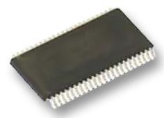
Features: • 18-bit bidirectional bus interface• 5V I/O Compatible• 3-State buffers• Output capability: +64mA/-32mA• TTL and LVTTL input and output switching levels• Bus-hold data inputs eliminate the need for external pull-up resistors to hold unused inputs̶...
74ALVT16501: Features: • 18-bit bidirectional bus interface• 5V I/O Compatible• 3-State buffers• Output capability: +64mA/-32mA• TTL and LVTTL input and output switching levels̶...
SeekIC Buyer Protection PLUS - newly updated for 2013!
268 Transactions
All payment methods are secure and covered by SeekIC Buyer Protection PLUS.
US $2 - 2.02 / Piece
Buffers & Line Drivers 16-Bit Buffer/Driver With 3-State Outputs
SYMBOL | PARAMETER | CONDITIONS | RATING | UNIT |
VCC | DC supply voltage | 0.5 to +4.6 | V | |
IIK | DC input diode current | VI < 0 | 50 | mA |
VI | DC input voltage3 | -0.5 to +7.0 | V | |
IOK | DC output diode current | VO < 0 | 50 | mA |
VOUT | DC output voltage3 | Output in Off or High state | -0.5 to +7.0 | V |
IOUT | DC output current |
output in Low state
|
128 |
mA |
output in High state | -64 | |||
Tstg | Storage temperature range | -65 to 150 | °C |
NOTES:
1. Stresses beyond those listed may cause permanent damage to the device. These are stress ratings only and functional operation of the device at these or any other conditions beyond those indicated under "recommended operating conditions" is not implied. Exposure to absolute-maximum-rated conditions for extended periods may affect device reliability.
2. The performance capability of a high-performance integrated circuit in conjunction with its thermal environment can create junction temperatures which are detrimental to reliability. The maximum junction temperature of this integrated circuit should not exceed 150°C.
3. The input and output negative voltage ratings may be exceeded if the input and output clamp current ratings are observed.
The 74ALVT16501 is a high-performance BiCMOS product designed for VCC operation at 2.5V and 3.3V with I/O compatibility up to 5V.
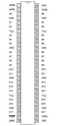
The 74ALVT16501 is an 18-bit universal transceiver featuring non-inverting 3-State bus compatible outputs in both send and receive directions. Data flow in each direction is controlled by output enable (OEAB and OEBA), latch enable (LEAB and LEBA), and clock (CPAB and CPBA) inputs. For A-to-B data flow, the device operates in the transparent mode when LEAB is High. When LEAB is Low, the A data of the 74ALVT16501 is latched if CPAB is held at a High or Low logic level. If LEAB
is Low, the A-bus data is stored in the latch/flip-flop on the Low-to-High transition of CPAB. When OEAB is High, the outputs are active. When OEAB is Low, the outputs are in the high-impedance state.
Data of the 74ALVT16501 flow for B-to-A is similar to that of A-to-B but uses OEBA, LEBA and CPBA. The output enables are complimentary (OEAB is active High, and OEBA is active Low).
Active bus-hold circuitry of the 74ALVT16501 is provided to hold unused or floating data inputs at a valid logic level.