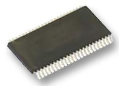
Features: ` 1.653.6V VCC supply operation` 3.6V tolerant inputs and outputs` 26 series resistors on both the A and B Port outputs.` tPD (A to B, B to A) 4.3 ns max for 3.0V to 3.6V VCC 5.1 ns max for 2.3V to 2.7V VCC 9.2 ns max for 1.65V to 1.95V VCC` Power-down HIGH impedance inputs and outputs` ...
74ALVCR162601: Features: ` 1.653.6V VCC supply operation` 3.6V tolerant inputs and outputs` 26 series resistors on both the A and B Port outputs.` tPD (A to B, B to A) 4.3 ns max for 3.0V to 3.6V VCC 5.1 ns max fo...
SeekIC Buyer Protection PLUS - newly updated for 2013!
268 Transactions
All payment methods are secure and covered by SeekIC Buyer Protection PLUS.
US $2 - 2.02 / Piece
Buffers & Line Drivers 16-Bit Buffer/Driver With 3-State Outputs
The 74ALVCR162601, 18-bit universal bus transceiver, combines D-type latches and D-type flip-flops to allow data flow in transparent, latched, and clocked modes.
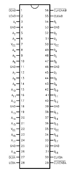
Data flow in each direction of the 74ALVCR162601 is controlled by output-enable (OEAB and OEBA), latch-enable (LEAB and LEBA), and clock (CLKAB and CLKBA) inputs. The clock can be controlled by the clock-enable (CLKENAB and CLKENBA) inputs. For A-to-B data flow, the device operates in the transparent mode when LEAB is HIGH. When LEAB is LOW, the A data is latched if CLKAB is held at a HIGH-to- LOW logic level. If LEAB is LOW, the A bus data is stored in the latch/flip-flop on the LOW-to-HIGH transition of CLKAB. Output-enable OEAB is active-LOW. When OEAB is HIGH, the outputs are in the high-impedance state. Data flow for B to A is similar to that of A to B but uses OEBA, LEBA,CLKBA andCLKENBA.
The 74ALVCR162601 is designed for low voltage (1.65V to 3.6V) VCC applications with I/O compatibility up to 3.6V. The 74ALVCR162601 is also designed with 26 series resistors on both the A and B Port outputs. This design reduces line noise in applications such as memory address drivers, clock drivers, and bus transceivers/transmitters.