74ALVCH16952

Features: • Complies with JEDEC standard no. 8-1A• CMOS low power consumption• MULTIBYTETM flow-through pin-out architecture• Low inductance, multiple center power and ground pins for minimum noise and ground bounce• Direct interface with TTL levels• Output driv...

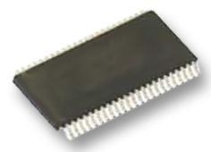
product image

74ALVCH16952 Picture
SeekIC No. : 004249451 Detail

74ALVCH16952: Features: • Complies with JEDEC standard no. 8-1A• CMOS low power consumption• MULTIBYTETM flow-through pin-out architecture• Low inductance, multiple center power and ground...

floor Price/Ceiling Price

Part Number:
74ALVCH16952
Supply Ability:
5000

Price Break

  • Qty
  • 1~5000
  • Unit Price
  • Negotiable
  • Processing time
  • 15 Days
Total Cost: $ 0.00

SeekIC Buyer Protection PLUS - newly updated for 2013!

  • Escrow Protection.
  • Guaranteed refunds.
  • Secure payments.
  • Learn more >>

Month Sales

268 Transactions

Rating

evaluate  (4.8 stars)

Upload time: 2024/5/19

Payment Methods

All payment methods are secure and covered by SeekIC Buyer Protection PLUS.

Notice: When you place an order, your payment is made to SeekIC and not to your seller. SeekIC only pays the seller after confirming you have received your order. We will also never share your payment details with your seller.
Product Details

Description


Features:

• Complies with JEDEC standard no. 8-1A
• CMOS low power consumption
• MULTIBYTETM flow-through pin-out architecture
• Low inductance, multiple center power and ground pins for minimum noise and ground bounce
• Direct interface with TTL levels
• Output drive capability 50W transmission lines @ 85°C


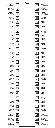
Pinout

  Connection Diagram


Specifications

SYMBOL
PARAMETER CONDITIONS
RATING
UNIT
VCC
DC supply voltage  
0.5 to +4.6
V
IIK
DC input diode current VI<0
-50
mA
VI
DC input voltage For control pins1
0.5 to +4.6
V
For data inputs1
0.5 to VCC +0.5
IOK
DC output diode current VO>VCC or VO<0
±50
mA
VO
DC output voltage Note 1
-50toVcc+0.5
V
IO
DC output source or sink current VO = 0 to VCC
±50
mA
IGND, ICC
DC VCC or GND current  
±100
mA
Tstg
Storage temperature range  
-65to+150
PTOT
Power dissipation per package
plastic medium-shrink (SSOP)
plastic thin-medium-shrink (TSSOP)
For temperature range: 40 to +125 °C
above +55°C derate linearly with 11.3 mW/
above +55°C derate linearly with 8 mW/K
850
600
m/W


Description

The 74ALVCH16952 consists of two sections, each containing a dual octal non-inverting registered transceiver. Two 8-bit back to back registers store data flowing in both directions between two bi-directional busses. Data applied to the inputs is entered and stored on the rising edge of the clock (CPXX, where X is AB or BA) provided that the clock enable (CEXX) is LOW. The data of the 74ALVCH16952 is then present at the 3-State output buffers, but is only accessible when the output enable input (OEXX) is LOW. Data flow from A inputs to B outputs is the same as for B inputs to A outputs.


Customers Who Bought This Item Also Bought

Margin,quality,low-cost products with low minimum orders. Secure your online payments with SeekIC Buyer Protection.
Inductors, Coils, Chokes
Optical Inspection Equipment
Motors, Solenoids, Driver Boards/Modules
LED Products
View more