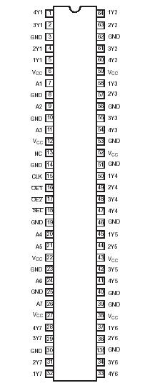
Features: • ESD protection exceeds 2000 V HBM per JESD22-A114, 200 V MM per JESD22-A115 and 1000 V CDM per JESD22-C101
• Latch-up testing is done to JESDEC Standard JESD78 which exceeds 100 mA
• Bus hold on data inputs eliminates the need for external pullup/pulldown resistorsPinout Specifications
|
SYMBOL |
PARAMETER |
CONDITIONS |
RATING |
UNIT |
|
VCC |
Supply voltage range |
|
0.5 to +4.6 |
V |
|
VI |
Input voltage range |
See Note 2 |
0.5 to +4.6 |
V |
|
VO |
Output voltage range |
See Notes 2 and 3 |
0.5 to VCC +0.5 |
V |
|
IIK |
Input clamp current |
VI < 0 |
50 |
mA |
|
IOK |
Output clamp current |
VO < 0 |
50 |
mA |
|
IO |
Continuous output current |
See Note 4 |
±50 |
mA |
|
ICC, IGND |
Continuous current through each VCC
or GND |
|
±100 |
mA |
|
JA |
Package thermal impedance |
See Note 4 |
106 |
°C/W |
|
Tstg |
Storage temperature range |
|
-65to+150 |
°C |
DescriptionThis 7 channel 1-bit to 4-bit address register/driver is designed for 2.3 V to 3.6 V VCC operation. This device is ideal for use in applications in which a single address bus is driving four separate memory locations. The 74ALVCH16832 can be used as a buffer or a register, depending on the logic level of the select (SEL) input.When SEL is a logic high, the device is in the buffer mode. The outputs follow the inputs and are controlled by the two output-enable(OE) inputs. Each OE controls two groups of seven outputs.When SEL is a logic low, the 74ALVCH16832 is in the register mode. The register is an edge-triggered D-type flip-flop. On the positive transition of the clock (CLK) input, data at the A inputs is stored in the internal registers. OE operates the same as in the buffer mode.When OE is a logic low, the outputs are in a normal logic state, (high or low logic level). When OE is a logic high, the outputs are in the high-impedance state.Neither SEL of OE affect the internal operation of the flip-flops. Old data can be retained or new data can be entered while the outputs are in the high-impedance state.
The three unique features of the 74ALVCH16832: The first one is ESD protection exceeds 2000 V HBM per JESD22-A114,200 V MM per JESD22-A115 and 1000 V CDM per JESD22-C101.The second one is latch-up testing is done to JESDEC Standard JESD78 which exceeds 100 mA.The third one is bus hold on data inputs eliminates the need for external pullup/pulldown resistors.
There are some absolute maximum ratings about the 74ALVCH16832.Supply voltage range(VCC) is0.5 V to +4.6 V.Input voltage range(VI) is 0.5 V to +4.6 V.Output voltage range(VO) is 0.5 V to VCC +0.5 V.Input clamp current(IIK,VI < 0) is50 mA.Output clamp current(IOK, VO < 0 ) is50 mA.Continuous output current(IO) is 50 mA.Storage temperature range(stg) is 65°C to +150°C.

 74ALVCH16832 Data Sheet


