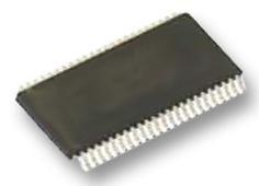
PinoutDescriptionThe 74ALVCH16271 is designed as 3.3V CMOS 12bit to 24-bit multiplexed bus exchanger with 3-state outputs and bus-hold. It is intended for applications in which two separate data paths must be multiplexed onto, or demultiplexed from, a single data path. This device is particularly ...
74ALVCH16271: PinoutDescriptionThe 74ALVCH16271 is designed as 3.3V CMOS 12bit to 24-bit multiplexed bus exchanger with 3-state outputs and bus-hold. It is intended for applications in which two separate data pat...
SeekIC Buyer Protection PLUS - newly updated for 2013!
268 Transactions
All payment methods are secure and covered by SeekIC Buyer Protection PLUS.
US $2 - 2.02 / Piece
Buffers & Line Drivers 16-Bit Buffer/Driver With 3-State Outputs
The 74ALVCH16271 is designed as 3.3V CMOS 12bit to 24-bit multiplexed bus exchanger with 3-state outputs and bus-hold. It is intended for applications in which two separate data paths must be multiplexed onto, or demultiplexed from, a single data path. This device is particularly suitable as an interface between conventional DRAMs and high-speed microprocessors.
The ten features of the 74ALVCH16271. (1) 0.5 MICRON CMOS technology. (2) Typical tSK(0) (output skew) < 250ps. (3) ESD > 2000V per MIL-STD-883, method 3015; and > 200V using machine model (C=200pF, R=0). (4) 0.635mm pitch SSOP, 0.50mm pitch TSSOP, and 0.40mm pitch TVSOP packages. (5) Extended commercial range of -40°C to + 85°C. (6) Vcc=3.3V ± 0.3V, normal range. (7) Vcc = 2.7V to 3.6V, extended range. (8) Vcc = 2.5V ± 0.2V. (9) CMOS power levels (0.4W typ static). (10) Rail-to-rail output swing for increased noise margin. That are all the main features.
Some absolute maximum ratings of the 74ALVCH16271 have been concluded into several points as follow. (1) Its terminal voltage with respect to GND would be from -0.5V to +4.6V. (2) Its terminal voltage with respect to GND would be from -0.5V to Vcc+0.5V. (3) Its storage temperature range would be from -65°C to +150°C. (4) Its DC output current would be from -50mA to 50mA. (5) Its continuous clamp current would be +/-50mA. (6) The continuous clamp current of the 74ALVCH16271, Vo<0 would be -50mA. (7) Its continuous current through each Vcc to GND would be +/-100mA. It should be noted that stresses greater than those listed under absolute maximum ratings may cause permanent damage to the 74ALVCH16271.
Also some DC electrical characteristics about 74ALVCH16271. (1) Its input high voltage level would be min 1.7V with condition of Vcc=2.3V to 2.7V and would be min 2.0V with condition of Vcc=2.7V to 3.6V. (2) Its input low voltage level would be max 0.7V with condition of Vcc=2.3V to 2.7V and would be max 0.8V with condition of Vcc=2.7V to 3.6V. (3) Its input high current and its input low current would be max +/-5uA. And so on. If you have any question or suggestion or want to know more information about the 74ALVCH16271 please contact us for details. Thank you!