Output Type
: 3-State
Logic Type
: CMOS
Supply Voltage - Max
: 3.6 V
Maximum Operating Temperature
: + 85 C
Output Level
: LVTTL
High Level Output Current
: - 24 mA
Low Level Output Current
: 24 mA
Supply Voltage - Min
: 1.65 V
Logic Family
: ALVC
Input Level
: LVTTL
Number of Channels per Chip
: 18
Propagation Delay Time
: 5.2 ns
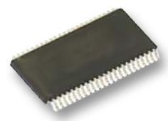
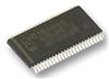
Package / Case
: TSSOP W
Packaging
: Rail
DescriptionThe 74ALVC16835MTD is a type of low voltage 18-bit universal bus driver which connects D-type latches and D-type flip-flops to accept data flow in transparent, latched and clocked modes.
Features of 74ALVC16835MTD are:(1)Compatible with PC100 DIMM module specifications; (2)1.65V to 3.6V VCC supp ly operation; (3)3.6V tolerant inputs and outputs; (4)tPD (CLK to On):4.5 ns max for 3.0V to 3.6V VCC,5.5 ns max for 2.3V to 2.7V VCC,9.2 ns max for 1.65V to 1.95V VCC; (5)Power-off high impedance inputs and outputs; (6)Supports live insertion/withdrawal (Note 1); (7)Latchup conforms to JEDEC JED78; (8)ESD performance:Human body model > 2000V,Machine model >200V.
The absolute maximum ratings and DC electrical characteristics of the 74ALVC16835MTD can be summarized as:(1): supply voltage is-0.5V to +4.6V;(2):DC input voltage is-0.5V to 4.6V;(3):output voltage is-0.5V to VCC +0.5V;(4):DC input diode current is-50mA when VI is less than 0V;(5):DC output diode current is-50mA when VO is less than 0V;(6):DC output source/sink current is±50 mA;(7):DC VCC or GND current is±100 mA per supply Pin;(8):storage tempe rature ranges from -65°C to +150°C.DC electrical characteristics:(1):input leakage current of the 74ALVC16835MTD is±5.0uA max when VI is between 0V and3.6V;(2):quiescent supply current is 40uA max when VI is VCC or GND,IO is 0;(3):increase in ICC per input is 750uA max when VIN is VCC-0.6V,etc.
 74ALVC16835MTD Data Sheet