DescriptionThe 74ALVC16601GX is a type of 18-bit universal bus transceiverwhich connects D-type latches and D-type flip-flops to ac cept data flow in transparent, latched, and clocked modes. Features of 74ALVC16601GX are:(1)1.65V3.6V VCC supply operation; (2)3.6V tolerant inputs and outputs; (3)t...
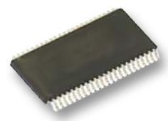
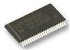
74ALVC16601GX: DescriptionThe 74ALVC16601GX is a type of 18-bit universal bus transceiverwhich connects D-type latches and D-type flip-flops to ac cept data flow in transparent, latched, and clocked modes. Featur...
SeekIC Buyer Protection PLUS - newly updated for 2013!
268 Transactions
All payment methods are secure and covered by SeekIC Buyer Protection PLUS.
US $2 - 2.02 / Piece
Buffers & Line Drivers 16-Bit Buffer/Driver With 3-State Outputs
The 74ALVC16601GX is a type of 18-bit universal bus transceiverwhich connects D-type latches and D-type flip-flops to ac cept data flow in transparent, latched, and clocked modes.
Features of 74ALVC16601GX are:(1)1.65V3.6V VCC supply operation; (2)3.6V tolerant inputs and outputs; (3)tPD (A to B, B to A):3.4 ns max for 3.0V to 3.6V VCC,4.0 ns max for 2.3V to 2.7V VCC,7.0 ns max for 1.65V 1.95V VCC; (4)power-down high impedance inputs and outputs; (5)supports live insertion/withdrawal (Note 1); (6)uses patented noise/EMI reduction circuitry; (7)latchup conforms to JEDEC JED78; (8)ESD performance:Human body model > 2000 V,Machine model >200V; (9)also packaged in plastic fine-pitch ball grid array(FBGA) (Preliminary).
The absolute maximum ratings and DC electrical characteristics of the 74ALVC16601GX can be summarized as:(1): supply voltage is-0.5V to +4.6V;(2):DC input voltage is-0.5V to 4.6V;(3):output voltage is-0.5V to VCC +0.5V;(4):DC input diode current is-50mA when VI is less than 0V;(5):DC output diode current is-50mA when VO is less than 0V;(6):DC output source/sink current is±50 mA;(7):DC VCC or GND current is ±100 mA per supply Pin;(8):storage tem perature ranges of the 74ALVC16601GX from -65°C to +150°C.DC electrical characteristics:(1):input leakage current is±5.0uA max when VI is between 0V and3.6V;(2):quiescent supply current is 40uA max when VI is VCC or GND,IO is 0;(3):increase in ICC per input is 750uA max when VIN is VCC-0.6V,etc.