Features: ` 1.65V3.6V VCC supply operation
` 3.6V tolerant inputs and outputs
` 26 series resistors in B-Port outputs
` tPD (A to B)
4.3 ns max for 3.0V to 3.6V VCC
5.1 ns max for 2.3V to 2.7V VCC
9.2 ns max for 1.65V to 1.95V VCC
` Power-down high impedance inputs and outputs
` Supports live insertion/withdrawal (Note 1)
` Uses patented noise/EMI reduction circuitry
` Latchup conforms to JEDEC JED78
` ESD performance:
Human body model > 2000V
Machine model >200V
Note 1: To ensure the high-impedance state during power up or power down, OE should be tied to VCC through a pull-up resistor; the minimum value of the resistor is determined by the current-sourcing capability of the driver.Pinout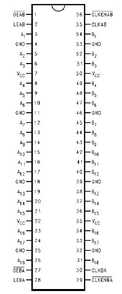 Specifications
Supply Voltage (VCC).............. −0.5V to +4.6V
DC Input Voltage (VI) .............. −0.5V to 4.6V
Output Voltage (VO) (Note 3) ....... −0.5V to VCC +0.5V
DC Input Diode Current (IIK)
VI < 0V .........................−50 mA
DC Output Diode Current (IOK)
VO < 0V ........................ −50 mA
DC Output Source/Sink Current
(IOH/IOL)........................ ±50 mA
DC VCC or GND Current per
Supply Pin (ICC or GND)............... ±100 mA
Storage Temperature Range (TSTG).... −65°C to +150°C
Note 5: The Absolute Maximum Ratings are those values beyond which the safety of the device cannot be guaranteed. The device should not be operated at these limits. The parametric values defined in the Electrical Characteristics tables are not guaranteed at the Absolute Maximum Ratings. The "Recommended Operating Conditions" table will define the conditions for actual device operation.
Note 6: IO Absolute Maximum Rating must be observed.
DescriptionThe 74ALVC162601, 18-bit universal bus transceiver, combines D-type latches and D-type flip-flops to allow data flow in transparent, latched, and clocked modes.
Data of the 74ALVC162601 flow in each direction is controlled by output-enable (OEAB and OEBA), latch-enable (LEAB and LEBA), and clock (CLKAB and CLKBA) inputs. The clock can be controlled by the clock-enable (CLKENAB and CLKENBA) inputs. For A-to-B data flow, the device operates in the transparent mode when LEAB is HIGH. When LEAB is LOW, the A data is latched if CLKAB is held at a HIGH-to- LOW logic level. If LEAB is LOW, the A bus data is stored in the latch/flip-flop on the LOW-to-HIGH transition of CLKAB. Output-enable OEAB is active-LOW. When OEAB is HIGH, the outputs are in the HIGH-impedance state. Data flow for B to A is similar to that of A to B but uses OEBA, LEBA, CLKBA and CLKENBA.
The 74ALVC162601 is designed for low voltage (1.65V to 3.6V) VCC applications with I/O compatibility up to 3.6V. The 74ALVC162601 is also designed with 26 series resistors in the B-Port outputs. This design reduces line noise in applications such as memory address drivers, clock drivers, and bus transceivers/transmitters.

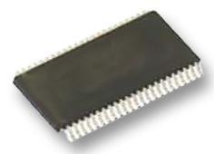
 74ALVC162601 Data Sheet