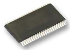
Features: • 74ALS563A is broadside pinout and inverting version of 74ALS373• 74ALS564A is broadside pinout and inverting version of 74ALS374• Inputs and outputs on opposite side of package allow easy interface to microprocessors• Useful as an input or output port for microp...
74ALS563A: Features: • 74ALS563A is broadside pinout and inverting version of 74ALS373• 74ALS564A is broadside pinout and inverting version of 74ALS374• Inputs and outputs on opposite side of...
SeekIC Buyer Protection PLUS - newly updated for 2013!
268 Transactions
All payment methods are secure and covered by SeekIC Buyer Protection PLUS.
US $2 - 2.02 / Piece
Buffers & Line Drivers 16-Bit Buffer/Driver With 3-State Outputs
SYMBOL | PARAMETER | RATING | UNIT |
VCC | Supply voltagee | 0.5 to+ 7 | V |
VIN | Input voltage | 0.5 to+ 7 | V |
IIN | Input current | 30 to +5 | mA |
VOUT | Voltage applied to output in High output state | 0.5 to VCC | V |
IOUT | Current applied to output in Low output state | 16 | mA |
Tamb | Operating free air temperature range | 0 to +70 | |
Tstg | Storage temperature range | 65 to 150 |
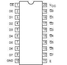
The 74ALS563A is an octal transparent latch coupled to eight 3-State output devices. The two sections of the device are controlled independently by enable (E) and output enable (OE) control gates.
The 74ALS563A is a complementary version of the 74ALS373 and has a broadside pinout configuration to facilitate PC board layout and allow easy interface with microprocessors.
The data of the 74ALS563A on the D inputs is transferred to the latch outputs when the enable (E) input is High. The latch remains transparent to the data input while E is High, and stores the inverted data that is present one setup time before the High-to-Low enable transition.
The 74ALS563A is a complementary version of the 74ALS373 and has a broadside pinout configuration to facilitate PC board layout and allow easy interface with microprocessors.
It is an 8-bit edge triggered register coupled to eight 3-State output buffers. The two sections of the device are controlled independently by clock (CP) and output enable (OE) control gates.
The register of the 74ALS563A is fully edge triggered. The state of the D input, one setup time before the Low-to-High clock transition is transferred to the corresponding flip-flop's Q output.
The active-Low output of the 74ALS563A enable (OE) controls all eight 3-State buffers independent of the latch operation. When OE is Low, latched or transparent data appears at the output.
When OE is High, the outputs are in high impedance "off" state, which means they will neither drive nor load the bus.