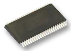
Features: • Ideal for addressable register applications• Enable for address and data synchronization applications• Eight edge-triggered D-type flip-flops• Buffered common clock• See 74ALS273 for master reset version• See 74ALS373 for transparent latch version...
74ALS377: Features: • Ideal for addressable register applications• Enable for address and data synchronization applications• Eight edge-triggered D-type flip-flops• Buffered common clo...
SeekIC Buyer Protection PLUS - newly updated for 2013!
268 Transactions
All payment methods are secure and covered by SeekIC Buyer Protection PLUS.
US $2 - 2.02 / Piece
Buffers & Line Drivers 16-Bit Buffer/Driver With 3-State Outputs
SYMBOL | PARAMETER | RATING | UNIT |
VCC | Supply voltagee | 0.5 to 7.0 | V |
VIN | Input current | 0.5 to 7.0 | V |
VIN | Input current | 30 to 5 | mA |
VOUT | Voltage applied to output in High output state | 0.5 to VCC | V |
IOUT | Current applied to output in Low output state | 48 | mA |
IOUT | Operating free air temperature range | 0 to +70 | |
Tstg | Storage temperature range | 65 to 150 |
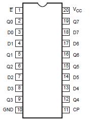
The 74ALS377 has eight edge-triggered D-type flip-flops with individual D inputs and Q outputs. The common buffered clock (CP) input loads all flip-flops simultaneously when the Enable (E) is Low.
The register of the 74ALS377 is fully edge-triggered. The state of each D input, one setup time before the Low-to-High clock transition, is transferred to the corresponding flip-flop's Q output. The E input must be stable one setup time prior to the Low-to-High clock transition for predictable operation.