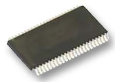
74ALS109A

PinoutSpecifications SYMBOL PARAMETER Value Unit VCC Supply voltage -0.5 to +7.0 V VIN Input voltage -0.5 to +7.0 V IIN Input current 30 to +5 mA VOUT Voltage applied to output in High output state -0.5 to VCC V IOUT Current applied to output in Low output stat...

product image

74ALS109A Picture
SeekIC No. : 004249266 Detail

74ALS109A: PinoutSpecifications SYMBOL PARAMETER Value Unit VCC Supply voltage -0.5 to +7.0 V VIN Input voltage -0.5 to +7.0 V IIN Input current 30 to +5 mA VOUT Voltage applied t...

floor Price/Ceiling Price

Part Number:
74ALS109A
Supply Ability:
5000

Price Break

  • Qty
  • 1~5000
  • Unit Price
  • Negotiable
  • Processing time
  • 15 Days
Total Cost: $ 0.00

SeekIC Buyer Protection PLUS - newly updated for 2013!

  • Escrow Protection.
  • Guaranteed refunds.
  • Secure payments.
  • Learn more >>

Month Sales

268 Transactions

Rating

evaluate  (4.8 stars)

Upload time: 2024/5/31

Payment Methods

All payment methods are secure and covered by SeekIC Buyer Protection PLUS.

Notice: When you place an order, your payment is made to SeekIC and not to your seller. SeekIC only pays the seller after confirming you have received your order. We will also never share your payment details with your seller.
Product Details

Description


Pinout

  Connection Diagram


Specifications

SYMBOL PARAMETER Value Unit
VCC Supply voltage -0.5 to +7.0 V
VIN Input voltage -0.5 to +7.0 V
IIN Input current 30 to +5 mA
VOUT Voltage applied to output in High output state -0.5 to VCC V
IOUT Current applied to output in Low output state 16 mA
Tamb Operating free-air temperature range 0 to +70
Tstg Storage Temperature -65 to +150


Description

The 74ALS109A is a dual positive edge-triggered JK-type flip-flop featuring individual J, K, clock, set, and reset inputs; also true and complementary outputs. Set (SD) and reset (RD) are asynchronous active-Low inputs and operate independently of the clock (CP) input. The J and K are edge-triggered inputs which control the state changes of the flip-flops as described in the function table. Clock triggering of the 74ALS109A occurs at a voltage level and is not directly related to the transition time of the positive-going pulse. The J and K inputs must be stable just one setup time prior to the Low-to-High transition of the clock for predictable operation. The JK design allows operation as a D flip-flop by tying J and K inputs together. Although the clock input is level sensitive, the positive transition of the clock pulse between the 0.8V and 2.0V levels should be equal to or less than the clock to output delay time for reliable operation.


Customers Who Bought This Item Also Bought

Margin,quality,low-cost products with low minimum orders. Secure your online payments with SeekIC Buyer Protection.
RF and RFID
Memory Cards, Modules
Computers, Office - Components, Accessories
Line Protection, Backups
LED Products
View more