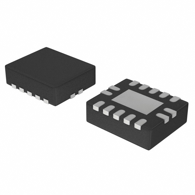
DescriptionThe 74AHCT541D belongs to 74AHC/AHCT541 family which are octal non-inverting buffer/line drivers with 3-state bus compatible outputs. The 3-state outputs are controlled by the output enable inputs OE0 and OE1. A HIGH on OEn causes the outputs to assume a high-impedance OFF-state. The 74...
74AHCT541D: DescriptionThe 74AHCT541D belongs to 74AHC/AHCT541 family which are octal non-inverting buffer/line drivers with 3-state bus compatible outputs. The 3-state outputs are controlled by the output enab...
SeekIC Buyer Protection PLUS - newly updated for 2013!
268 Transactions
All payment methods are secure and covered by SeekIC Buyer Protection PLUS.
The 74AHCT541D belongs to 74AHC/AHCT541 family which are octal non-inverting buffer/line drivers with 3-state bus compatible outputs. The 3-state outputs are controlled by the output enable inputs OE0 and OE1. A HIGH on OEn causes the outputs to assume a high-impedance OFF-state. The 74AHC/AHCT541 is a high-speed Si-gate CMOS device.
The features of 74AHCT541D can be summarized as (1)ESD protection: HBM EIA/JESD22-A114-A, exceeds 2000 V, MM EIA/JESD22-A115-A, exceeds 200 V, CDM EIA/JESD22-C101, exceeds 1000 V; (2)balanced propagation delays; (3)all inputs have a schmitt-trigger action; (4)inputs accepts voltages higher than VCC; (5)for AHC only: operates with CMOS input levels; (6)for AHCT only: operates with TTL input levels; (7)specified from -40 to +85°C and +125 °C.
The absolute maximum ratings of 74AHCT541D are (1)VCC DC supply voltage: -0.5 to +7.0V; (2)VI input voltage range: -0.5 to +7.0V; (3)IIK DC input diode current(VI < -0.5 V; note 1): -20mA; (4)IOK DC output diode current(VO < -0.5 V or VO > VCC + 0.5 V; note 1): ±20mA; (5)IO DC output source or sink current(-0.5 V < VO < VCC + 0.5 V): ±25 mA; (6)ICC DC VCC or GND current: ±75mA; (7)Tstg storage temperature range: -65 to +150°C; (8)PD power dissipation per package(for temperature range: -40 to +125 °C; note 2): 500mW(1. The input and output voltage ratings of the 74AHCT541D may be exceeded if the input and output current ratings are observed. 2. For SO packages: above 70 °C the value of PD derates linearly with 8 mW/K. For TSSOP packages: above 60 °C the value of PD derates linearly with 5.5 mW/K.)