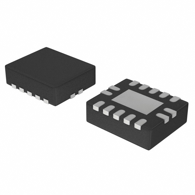
Number of Circuits
: 1
Maximum Operating Temperature
: + 125 C
Mounting Style
: SMD/SMT
Supply Voltage - Max
: 5.5 V
Polarity
: Non-Inverting
Input Type
: Single-Ended
Output Type
: Single-Ended
Packaging
: Tube
Low Level Output Current
: 8 mA
Package / Case
: SOT-163
Logic Type
: D-Type Edge Triggered Flip-Flop
High Level Output Current
: - 8 mA
Logic Family
: AHC
Propagation Delay Time
: 4.2 ns at 5 V
DescriptionThe 74AHC273D belongs to 74AHC/AHCT273 family which are high-speed Si-gate CMOS devices and are pin compatible with low power Schottky TTL (LSTTL). They are specified in compliance with JEDEC standard no. 7A. The state of each D input, one set-up time before the LOW-to-HIGH clock transition, is transferred to the corresponding output (Qn) of the flip-flop. All outputs will be forced LOW independently of clock or data inputs by a LOW on the MR input. The device is useful for applications where the true output only is required and the clock and master reset are common to all storage elements. The 74AHC/AHCT273 have eight edge-triggered, D-type flip-flops with individual D inputs and Q outputs. The common clock (CP) and master reset (MR) inputs load and reset (clear) all flip-flops simultaneously.
The absolute maximum ratings of 74AHC273D are (1)ideal buffer for MOS microcontroller or memory; (2)common clock and master reset; (3)ESD protection: HBM EIA/JESD22-A114-A exceeds 2000 V, MM EIA/JESD22-A115-A exceeds 200 V, CDM EIA/JESD22-C101 exceeds 1000 V; (4)balanced propagation delays; (5)all inputs have schmitt trigger actions; (6)inputs accepts voltages higher than VCC; (7)see '377' for clock enable version; (8)see '373' for transparent latch version; (9)see '374' for 3-state version; (10)for AHC only: operates with CMOS input levels; (11)for AHCT only: operates with TTL input levels; (12)specified from -40 to +85 °C and -40 to +125 °C.
The absolute maximum ratings of 74AHC273D are (1)VCC DC supply voltage: -0.5 to +7.0V; (2)VI input voltage range: -0.5 to +7.0V; (3)IIK DC input diode current(VI < -0.5 V; note 1): -20mA; (4)IOK DC output diode current(VO < -0.5 V or VO > VCC + 0.5 V; note 1): ±20mA; (5)IO DC output source or sink current(-0.5 V < VO < VCC + 0.5 V): ±25 mA; (6)ICC DC VCC or GND current of the 74AHC273D: ±75mA; (7)Tstg storage temperature range: -65 to +150°C; (8)PD power dissipation per package(for temperature range: -40 to +125 °C; note 2): 500mW(1. The input and output voltage ratings may be exceeded if the input and output current ratings are observed. 2. For SO packages: above 70 °C the value of PD derates linearly with 8 mW/K. For TSSOP packages: above 60 °C the value of PD derates linearly with 5.5 mW/K.)

 74AHC273D Data Sheet


