74AHC259

Features: · ESD protection:HBM EIA/JESD22-A114-A exceeds 2000 VMM EIA/JESD22-A115-A exceeds 200 VCDM EIA/JESD22-C101 exceeds 1000 V· Balanced propagation delays· All inputs have Schmitt-trigger actions· Combines demultiplexer and 8-bit latch· Serial-to-parallel capability· Output from each storage...

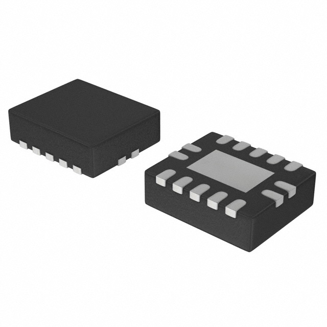
product image

74AHC259 Picture
SeekIC No. : 004249180 Detail

74AHC259: Features: · ESD protection:HBM EIA/JESD22-A114-A exceeds 2000 VMM EIA/JESD22-A115-A exceeds 200 VCDM EIA/JESD22-C101 exceeds 1000 V· Balanced propagation delays· All inputs have Schmitt-trigger acti...

floor Price/Ceiling Price

Part Number:
74AHC259
Supply Ability:
5000

Price Break

  • Qty
  • 1~5000
  • Unit Price
  • Negotiable
  • Processing time
  • 15 Days
Total Cost: $ 0.00

SeekIC Buyer Protection PLUS - newly updated for 2013!

  • Escrow Protection.
  • Guaranteed refunds.
  • Secure payments.
  • Learn more >>

Month Sales

268 Transactions

Rating

evaluate  (4.8 stars)

Upload time: 2024/12/25

Payment Methods

All payment methods are secure and covered by SeekIC Buyer Protection PLUS.

Notice: When you place an order, your payment is made to SeekIC and not to your seller. SeekIC only pays the seller after confirming you have received your order. We will also never share your payment details with your seller.
Product Details

Description


Features:

· ESD protection:
 HBM EIA/JESD22-A114-A exceeds 2000 V
 MM EIA/JESD22-A115-A exceeds 200 V
 CDM EIA/JESD22-C101 exceeds 1000 V
· Balanced propagation delays
· All inputs have Schmitt-trigger actions
· Combines demultiplexer and 8-bit latch
· Serial-to-parallel capability
· Output from each storage bit available
· Random (addressable) data entry
· Easily expandable
· Common reset input
· Useful as a 3-to-8 active HIGH decoder
· Inputs accept voltages higher than VCC
· For AHC only: operates with CMOS input levels
· For AHCT only: operates with TTL input levels
· Specified from -40 to +85 °C and from -40 to +125 °C.


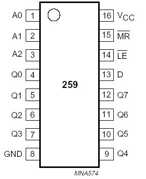
Pinout

  Connection Diagram


Specifications

Symbol
PARAMETER
CONDITIONS
MIN.
MAX.
UNIT
VCC
DC supply voltage
-0.5
+7.0
V
VI input voltage  
-0.5
+7.0
V
IIK DC input diode current VI < -0.5 V; note 1
-
-20
mA
IOK DC output clamping diode current VO < -0.5 V or VO > VCC + 0.5 V; note 1
-
±20
mA
IO DC output sink current -0.5 V < VO < VCC + 0.5 V
-
±25
mA
ICC DC VCC or GND current  
-
±75
mA
Tstg storage temperature  
-65
+150
°C
PD power dissipation per package for temperature range: -40 to +125 °C; note 2
-
500
mW
Notes
1. The input and output voltage ratings may be exceeded if the input and output current ratings are observed.
2. For SO packages: above 70 °C the value of PD derates linearly with 8 mW/K.
For TSSOP packages: above 60 °C the value of PD derates linearly with 5.5 mW/K.


Description

The 74AHC259 are high-speed Si-gate CMOS devices and are pin compatible with Low power Schottky TTL (LSTTL). They are specified in compliance with JEDEC standard No. 7A.

The 74AHC259 are high-speed 8-bit addressable latches designed for general purpose storage applications in digital systems. The '259' are multifunctional devices capable of storing single-line data in eight addressable latches, and also 3-to-8 decoder and demultiplexer, with active HIGH outputs (Q0 to Q7), functions are available.

The '259' also incorporates an active LOW common reset (MR) for resetting all latches as well as an active LOW enable input (LE).

The '259' has four modes of operation as shown in the mode select table. In the addressable latch mode, data on the data line (D) is written into the addressed latch. The addressed latch will follow the data input with all nonaddressed latches remaining in their previous states. In the memory mode, all latches remain in their previous states and are unaffected by the data or address inputs. In the 3-to-8 decoding or demultiplexing mode, the addressed output follows the state of the (D) input with all other outputs in the LOW state.

In the reset mode all outputs of the 74AHC259 are LOW and unaffected by the address (A0 to A2) and data (D) input. When operating the '259' as an address latch, changing more than one bit of the address could impose a transient-wrong address. Therefore, this should only be done while in the memory mode.

The mode select table summarizes the operations of the '259'.


Customers Who Bought This Item Also Bought

Margin,quality,low-cost products with low minimum orders. Secure your online payments with SeekIC Buyer Protection.
Prototyping Products
DE1
Tapes, Adhesives
803
Isolators
RF and RFID
Memory Cards, Modules
Circuit Protection
View more