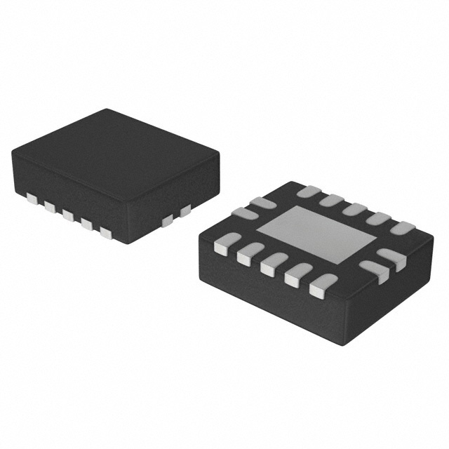
DescriptionThe 74AHC157PWDH is one member of the 74AHC157 series.The 74AHC157 is a high-speed Si-gate CMOS device and is pin compatible with low power Schottky TTL (LSTTL).The74AHC157 is quad 2-input multiplexer which selects 4 bits of data from two sources under the control of a common data selec...
74AHC157PWDH: DescriptionThe 74AHC157PWDH is one member of the 74AHC157 series.The 74AHC157 is a high-speed Si-gate CMOS device and is pin compatible with low power Schottky TTL (LSTTL).The74AHC157 is quad 2-inpu...
SeekIC Buyer Protection PLUS - newly updated for 2013!
268 Transactions
All payment methods are secure and covered by SeekIC Buyer Protection PLUS.
The 74AHC157PWDH is one member of the 74AHC157 series.The 74AHC157 is a high-speed Si-gate CMOS device and is pin compatible with low power Schottky TTL (LSTTL).The74AHC157 is quad 2-input multiplexer which selects 4 bits of data from two sources under the control of a common data select input (S). The enable input (E) is active LOW.When E is HIGH,all of the outputs(1Y to 4Y) are forced LOW regardless of all other input conditions.
Features of the 74AHC157PWDH are:(1)balanced propagation delays; (2)all inputs have schmitt-trigger actions; (3)multiple input enable for easy expansion; (4)ideal for memory chip select decoding; (5)inputs accept voltages higher than VCC; (6)for AHC only: operates with CMOS input levels; (7)for AHCT only: operates with TTL input levels; (8)specified from -40 to +85 and +125 .The device is useful for implementing highly irregular logic by generating any four of the 16 different functions of two variables with one variable common.Conventional single wave soldering of the 74AHC157PWDH is not recommended for surface mount devices(SMDs) or printed-circuit boards with a high component density, as solder bridging and non-wetting can present major problems.
The absolute maximum ratings of the 74AHC157PWDH can be summarized as:(1)DC supply voltage:-0.5 to 7.0V;(2)input voltage range:-0.5 to 7.0V;(3)DC Vcc or GND current:±75mA;(4)DC input diode current:-20mA; (5)DC output diode current:±20mA; (6)DC output source or sink current:±25mA; (7)storage temperature range:-65 to 150;(8)power dissipation per package:500mW.Reflow soldering requires solder paste (a suspension of fine solder particles, flux and binding agent) to be applied to the printed-circuit board by screen printing,stencilling or pressure-syringe dispensing before package placement. Several methods exist for reflowing; for example,infrared/convection heating in a conveyor type oven.Throughput times(preheating,soldering and cooling) vary between 100 and 200 seconds depending on heating method.During placement and before soldering,the package must be fixed with a droplet of adhesive. The adhesive can be applied by screen printing, pin transfer or syringe dispensing. The package of the 74AHC157PWDH can be soldered after the adhesive is cured.