74ACT899

Features: `Latchable transceiver with output sink of 24 mA`Option to select generate parity and check or feed-through data/parity in directions A-to-B or B-to-A`Independent latch enable for A-to-B and B-to-A directions`Select pin for ODD/EVEN parity`ERRA and ERRB output pins for parity checking`A...

product image

74ACT899 Picture
SeekIC No. : 004249098 Detail

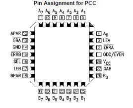
74ACT899: Features: `Latchable transceiver with output sink of 24 mA`Option to select generate parity and check or feed-through data/parity in directions A-to-B or B-to-A`Independent latch enable for A-to-B ...

floor Price/Ceiling Price

Part Number:
74ACT899
Supply Ability:
5000

Price Break

  • Qty
  • 1~5000
  • Unit Price
  • Negotiable
  • Processing time
  • 15 Days
Total Cost: $ 0.00

SeekIC Buyer Protection PLUS - newly updated for 2013!

  • Escrow Protection.
  • Guaranteed refunds.
  • Secure payments.
  • Learn more >>

Month Sales

268 Transactions

Rating

evaluate  (4.8 stars)

Upload time: 2024/7/15

Payment Methods

All payment methods are secure and covered by SeekIC Buyer Protection PLUS.

Notice: When you place an order, your payment is made to SeekIC and not to your seller. SeekIC only pays the seller after confirming you have received your order. We will also never share your payment details with your seller.
Product Details

Description


Features:

`Latchable transceiver with output sink of 24 mA
`Option to select generate parity and check or"feed-through" data/parity in directions A-to-B or B-to-A
`Independent latch enable for A-to-B and B-to-A directions
`Select pin for ODD/EVEN parity
`ERRA and ERRB output pins for parity checking
`Ability to simultaneously generate and check parity
`May be used in system applications in place of the 280
`May be used in system applications in place of the 657 and 373 (no need to change T/R to check parity)


Pinout

  Connection Diagram


Specifications

Supply Voltage (VCC) . . . . .. . -0.5V to +7.0V
DC Input Diode Current (IIK)
  VI = -0.5V . . . . .. . . . .. . . . .. -20 mA
  VI = VCC + 0.5V . . . . .. . . . .. . . +20 mA
DC Input Voltage (VI) . . . .-0.5V to VCC + 0.5V
DC Output Diode Current (IOK)
  VO = -0.5V . . . . .. . . . .. . . . .. -20 mA
  VO = VCC + 0.5V . . . . .. . . . .. . . +20 mA
DC Output Voltage (VO) . . . -0.5V to VCC + 0.5V
DC Output Source
  or Sink Current (IO). . . . .. . . . . ±50 mA
DC VCC or Ground Current
  per Output Pin (ICC or IGND) . . . . . ±50 mA
Storage Temperature (TSTG). .  -65°C to +150°C
DC Latch-Up Source or
  Sink Current . . . . .. . . . . . . . ±300 mA
Junction Temperature (TJ)  . . . .. . .  .140°C


Description

The 74ACT899 is a 9-bit to 9-bit parity transceiver with transparent latches. The device can operate as a feed-through transceiver or it can generate/check parity from the 8-bit data busses in either direction. The 74ACT899 features independent latch enables for the A-to-B direction and the B-to- A direction, a select pin for ODD/EVEN parity, and separate error signal output pins for checking parity.


Customers Who Bought This Item Also Bought

Margin,quality,low-cost products with low minimum orders. Secure your online payments with SeekIC Buyer Protection.
Static Control, ESD, Clean Room Products
Crystals and Oscillators
Optoelectronics
Cables, Wires - Management
Programmers, Development Systems
View more