74ACT715-R

Features: Maximum Input Clock Frequency > 130 MHzInterlaced and non-interlaced formats availableSeparate or composite horizontal and vertical Sync and Blank signals availableComplete control of pulse width via register programmingAll inputs are TTL compatible8 mA drive on all outputsDefault RS1...

product image

74ACT715-R Picture
SeekIC No. : 004249084 Detail

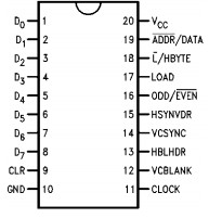
74ACT715-R: Features: Maximum Input Clock Frequency > 130 MHzInterlaced and non-interlaced formats availableSeparate or composite horizontal and vertical Sync and Blank signals availableComplete control of p...

floor Price/Ceiling Price

Part Number:
74ACT715-R
Supply Ability:
5000

Price Break

  • Qty
  • 1~5000
  • Unit Price
  • Negotiable
  • Processing time
  • 15 Days
Total Cost: $ 0.00

SeekIC Buyer Protection PLUS - newly updated for 2013!

  • Escrow Protection.
  • Guaranteed refunds.
  • Secure payments.
  • Learn more >>

Month Sales

268 Transactions

Rating

evaluate  (4.8 stars)

Upload time: 2024/6/12

Payment Methods

All payment methods are secure and covered by SeekIC Buyer Protection PLUS.

Notice: When you place an order, your payment is made to SeekIC and not to your seller. SeekIC only pays the seller after confirming you have received your order. We will also never share your payment details with your seller.
Product Details

Description


Features:

Maximum Input Clock Frequency > 130 MHz
Interlaced and non-interlaced formats available
Separate or composite horizontal and vertical Sync and Blank signals available
Complete control of pulse width via register  programming
All inputs are TTL compatible
8 mA drive on all outputs
Default RS170/NTSC values mask programmed into registers
ACT715-R is mask programmed to default to a Clock Enable state for easier start-up into 14.31818 MHz RS170 timing


Pinout

  Connection Diagram


Specifications

Supply Voltage (VCC) ......................... -0.5V to + 7.0V
DC Input Diode Current (IIK)
    VI = 0.5V .....................................................-20 mA
    VI = VCC + 0.5V ..........................................+20 mA
DC Input Voltage (VI) ..................-0.5V to VCC + 0.5V
DC Output Diode Current (IOK)
    VO = 0.5V ....................................................-20 mA
    VO = VCC +0.5V ..........................................+20 mA
DC Output Voltage (VO)................ -0.5V to VCC+0.5V
DC Output Source
    or Sink Current (IO) ....................................±15 mA
DC VCC or Ground Current
    per Output Pin (ICC or IGND) ......................±20 mA
Storage Temperature(TSTG)............ -65oC to +150oC
Junction Temperature (TJ)
    PDIP............................................................ 140oC

Supply Voltage (VCC)..............................4.5V to 5.5V
Input Voltage (VI).......................................0V to VCC
Output Voltage (VO)....................................0V to VCC
Operating Temperature (TA) .............-40oC to +85oC
Minimum Input Edge Rate (V/t)
    ACT Devices
    VIN from 30% to 70% of VCC
    VCC @ 3.3V, 4.5V, 5.5V......................... 125 mV/ns
Note 1: Absolute maximum ratings are those values beyond which damage to the device may occur. The databook specifications should be met, without exception, to ensure that the system design is reliable over its power supply, temperature, and output/input loading variables. Fairchild does not recommend operation of FACT™ circuits outside databook specifications.


Description

The 74ACT715-R is 20-pin TTL-input compatible devices capable of generating Horizontal, Vertical and Composite Sync and Blank signals for televisions and monitors. All pulse widths are completely definable by the user. The devices are capable of generating signals for both interlaced and noninterlaced modes of operation. Equalization and serration pulses can be introduced into the Composite Sync signal when needed.

Four additional signals of the 74ACT715-R can also be made available when Composite Sync or Blank are used. These signals can be used to generate horizontal or vertical gating pulses, cursor position or vertical Interrupt signal.

The 74ACT715-R make no assumptions concerning the system architecture. Line rate and field/frame rate are all a function of the values programmed into the data registers, the status register, and the input clock frequency.

The 74ACT715-R is mask programmed to default to a Clock Disable state. Bit 10 of the Status Register, Register 0, defaults to a logic "0". This facilitates (re)programming before operation.

The 74ACT715-R is the same as the ACT715 in all respects except that the 74ACT715-R is mask programmed to default to a Clock Enabled state. Bit 10 of the Status Register defaults to a logic "1". Although completely (re)programmable, the 74ACT715-R version is better suited for applications using the default 14.31818 MHz RS-170 register values. This feature allows power-up directly into operation, following a single CLEAR pulse.


Customers Who Bought This Item Also Bought

Margin,quality,low-cost products with low minimum orders. Secure your online payments with SeekIC Buyer Protection.
Undefined Category
Cables, Wires - Management
Potentiometers, Variable Resistors
Boxes, Enclosures, Racks
Tapes, Adhesives
803
Fans, Thermal Management
View more