74ACT533

Features: · ICC and IOZ reduced by 50%· Eight latches in a single package·3-STATE outputs drive bus lines or buffer memory address registers· Outputs source/sink 24 mA· Inverted version of the ACT373· TTL-compatible inputsPinoutSpecificationsSupply Voltage (VCC)........ - 0.5V to + 7.0VDC Input Di...

product image

74ACT533 Picture
SeekIC No. : 004249073 Detail

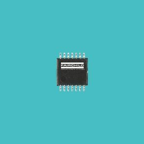
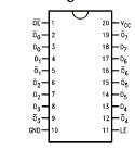
74ACT533: Features: · ICC and IOZ reduced by 50%· Eight latches in a single package·3-STATE outputs drive bus lines or buffer memory address registers· Outputs source/sink 24 mA· Inverted version of the ACT37...

floor Price/Ceiling Price

Part Number:
74ACT533
Supply Ability:
5000

Price Break

  • Qty
  • 1~5000
  • Unit Price
  • Negotiable
  • Processing time
  • 15 Days
Total Cost: $ 0.00

SeekIC Buyer Protection PLUS - newly updated for 2013!

  • Escrow Protection.
  • Guaranteed refunds.
  • Secure payments.
  • Learn more >>

Month Sales

268 Transactions

Rating

evaluate  (4.8 stars)

Upload time: 2024/5/31

Payment Methods

All payment methods are secure and covered by SeekIC Buyer Protection PLUS.

Notice: When you place an order, your payment is made to SeekIC and not to your seller. SeekIC only pays the seller after confirming you have received your order. We will also never share your payment details with your seller.
Product Details

Description


Features:

· ICC and IOZ reduced by 50%
· Eight latches in a single package
·3-STATE outputs drive bus lines or buffer memory address registers
· Outputs source/sink 24 mA
· Inverted version of the ACT373
· TTL-compatible inputs


Pinout

  Connection Diagram


Specifications

Supply Voltage (VCC)........ - 0.5V to + 7.0V
DC Input Diode Current (IIK)
VI = - 0.5V .................- 20 mA
VI = VCC + 0.5V ..............+ 20 mA
DC Input Voltage (VI)..... -0.5V to VCC + 0.5V
DC Output Diode Current (IOK)
VO = - 0.5V................. - 20 mA
VO = VCC + 0.5V ..............+ 20 mA
DC Output Voltage (VO) ....- 0.5V to VCC + 0.5V
DC Output Source
or Sink Current (IO) ...... ......± 50 mA
DC VCC or Ground Current
per Output Pin (ICC or IGND) ........± 50 mA
Storage Temperature (TSTG) ..- 65°C to + 150°C
DC Latchup Source
or Sink Current ..............± 300 mA
Junction Temperature (TJ)
PDIP .....................140°C
Supply Voltage (VCC).......... 4.5V to 5.5V
Input Voltage (VI)............. 0V to VCC
Output Voltage (VO)............ 0V to VCC
Operating Temperature (TA).... -40°C to +85°C
Minimum Input Edge Rate DV/Dt
VIN from 0.8V to 2.0V
VCC @ 4.5V, 5.5V............ . 125 mV/ns

Note 1: Absolute maximum ratings are those values beyond which damage to the device may occur. The databook specifications should be met, without exception, to ensure that the system design is reliable over its power supply, temperature, and output/input loading variables. Fairchild does not recommend operation of FACTä circuits outside databook specifications.


Description

The 74ACT533 consists of eight latches with 3-STATE outputs for bus organized system applications. The flip-flops appear transparent to the data when Latch Enable (LE) is HIGH. When LE is low, the data satisfying the input timing requirements is latched. Data of the 74ACT533 appears on the bus when the Output Enable (OE) is LOW. When OE is HIGH, the bus output is in the high impedance state.


Customers Who Bought This Item Also Bought

Margin,quality,low-cost products with low minimum orders. Secure your online payments with SeekIC Buyer Protection.
RF and RFID
Audio Products
Computers, Office - Components, Accessories
Batteries, Chargers, Holders
Soldering, Desoldering, Rework Products
Hardware, Fasteners, Accessories
View more