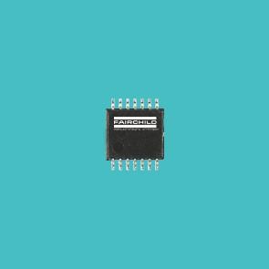
74ACT16657

Features: Members of the Texas Instruments Widebus™ FamilyInputs Are TTL-Voltage CompatibleFlow-Through Architecture Optimizes PCB LayoutDistributed VCC and GND Pin Configuration Minimizes High-Speed Switching NoiseEPIC™ (Enhanced-Performance Implanted CMOS) 1-µm Process500-mA Ty...

product image

74ACT16657 Picture
SeekIC No. : 004249036 Detail

74ACT16657: Features: Members of the Texas Instruments Widebus™ FamilyInputs Are TTL-Voltage CompatibleFlow-Through Architecture Optimizes PCB LayoutDistributed VCC and GND Pin Configuration Minimizes Hig...

floor Price/Ceiling Price

Part Number:
74ACT16657
Supply Ability:
5000

Price Break

  • Qty
  • 1~5000
  • Unit Price
  • Negotiable
  • Processing time
  • 15 Days
Total Cost: $ 0.00

SeekIC Buyer Protection PLUS - newly updated for 2013!

  • Escrow Protection.
  • Guaranteed refunds.
  • Secure payments.
  • Learn more >>

Month Sales

268 Transactions

Rating

evaluate  (4.8 stars)

Upload time: 2024/11/21

Payment Methods

All payment methods are secure and covered by SeekIC Buyer Protection PLUS.

Notice: When you place an order, your payment is made to SeekIC and not to your seller. SeekIC only pays the seller after confirming you have received your order. We will also never share your payment details with your seller.
Product Details

Description


Features:

Members of the Texas Instruments Widebus™ Family
Inputs Are TTL-Voltage Compatible
Flow-Through Architecture Optimizes PCB Layout
Distributed VCC and GND Pin Configuration Minimizes High-Speed Switching Noise
EPIC™ (Enhanced-Performance Implanted CMOS) 1-µm Process
500-mA Typical Latch-Up Immunity at 125°C
Package Options Include Plastic 300-mil Shrink Small-Outline (DL) Packages Using 25-mil Center-to-Center Pin Spacings and 380-mil
Fine-Pitch Ceramic Flat (WD) Packages Using 25-mil Center-to-Center Pin Spacings


Pinout

  Connection Diagram


Specifications

Supply voltage range, VCC   . . . . . . . . . . . . . . . . . . . . . . . . . . . . . . . . . . . . . . . . . . .0.5 V to 7 V
Input voltage range, VI (see Note 1)   . . . . . . . . . . . . . . . . . . . . . . . . .  . . .0.5 V to VCC + 0.5 V
Output voltage range, VO (see Note 1)   . . . . . . . . . . . . . . . . . . . . . .. . . . .0.5 V to VCC + 0.5 V
Input clamp current, IIK (VI < 0 or VI > VCC)  . . . . . . . . . . . . . . . . . . . . . . . . . . . . . . . . . .±20 mA
Output clamp current, IOK (VO < 0 or VO > VCC)  . . . . . . . . . . . . . . . . . . . . . . . . . . . .  . . .±50 mA
Continuous output current, IO (VO = 0 to VCC)  . . . . . . . . . . . . . . . . . . . . . . . . . . . . . . . .±50 mA
Continuous current through VCC or GND  . . . . . . . . . . . . . . . . . . . . . . . . . . . . . . . . . . . .±500 mA
Maximum package power dissipation at TA = 55°C (in still air) (see Note 2): DL package. .1.4 W
Storage temperature range, Tstg  . . . . . . . . . . . . . . . . . . . . . . . . . . . . . . . . . . . .65°C to 150°C
Stresses beyond those listed under "absolute maximum ratings" may cause permanent damage to the device. These are stress ratings only, and functional operation of the device at these or any other conditions beyond those indicated under "recommended operating conditions" is not implied. Exposure to absolute-maximum-rated conditions for extended periods may affect device reliability.
NOTES: 1. The input and output voltage ratings may be exceeded if the input and output current ratings are observed.
             2. The maximum package power dissipation is calculated using a junction temperature of 150oC and a board trace length of 750 mils.


Description

The 74ACT16657 contain two noninverting octal transceiver sections with separate parity generator/checker circuits and control signals. For either section, the transmit/receive (1T/R or 2T/R) input determines the direction of data flow. When 1T/R (or 2T/R) is high, data flows from the 1A (or 2A) port to the 1B (or 2B) port (transmit mode); when 1T/R (or 2T/R) is low, data flows from the 1B (or 2B) port to the 1A (or 2A) port (receive mode). When the output-enable (1OE or 2OE) input is high, both the 1A (or 2A) and 1B (or 2B) ports are in the high-impedance state.

Odd or even parity of the 74ACT16657 is selected by a logic high or low level, respectively, on the 1ODD/EVEN (or 2ODD/EVEN) input. 1PARITY (or 2PARITY) carries the parity bit value; it is an output from the parity generator/checker in the transmit mode and an input to the parity generator/checker in the receive mode.

In the transmit mode of the 74ACT16657, after the 1A (or 2A) bus is polled to determine the number of high bits, 1PARITY (or 2PARITY) is set to the logic level that maintains the parity sense selected by the level at the 1ODD/EVEN (or 2ODD/EVEN) input. For example, if 1ODD/EVEN is low (even parity selected) and there are five high bits on the 1A bus, then 1PARITY is set to the logic high level so that an even number of the nine total bits (eight 1A-bus bits plus parity bit) are high.

In the receive mode, after the 1B (or 2B) bus is polled to determine the number of high bits, the 1ERR (or 2ERR) output logic level indicates whether or not the data to be received exhibits the correct parity sense. For example, if 1ODD/EVEN is high (odd parity selected), 1PARITY is high, and there are three high bits on the 1B bus, then 1ERR is low, indicating a parity error.

The 74ACT16657 is packaged in TI's shrink small-outline package, which provides twice the I/O pin count and functionality of standard small-outline packages in the same printed-circuit-board area.

The 74ACT16657 is characterized for operation over the full military temperature range of 55°C to 125°C. The 74ACT16657 is characterized for operation from 40°C to 85°C.


Customers Who Bought This Item Also Bought

Margin,quality,low-cost products with low minimum orders. Secure your online payments with SeekIC Buyer Protection.
Discrete Semiconductor Products
Line Protection, Backups
Integrated Circuits (ICs)
Cables, Wires - Management
Optical Inspection Equipment
View more