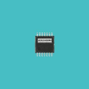
DescriptionThe 74ACT11240 is designed as octal buffer or line driver specifically to improve both the performance and density of 3-state memory address drivers, clock drivers, and bus-oriented receivers and transmitters. This device provides inverting outputs and symmetrical active-low output-enab...
74ACT11240: DescriptionThe 74ACT11240 is designed as octal buffer or line driver specifically to improve both the performance and density of 3-state memory address drivers, clock drivers, and bus-oriented recei...
SeekIC Buyer Protection PLUS - newly updated for 2013!
268 Transactions
All payment methods are secure and covered by SeekIC Buyer Protection PLUS.
The 74ACT11240 is designed as octal buffer or line driver specifically to improve both the performance and density of 3-state memory address drivers, clock drivers, and bus-oriented receivers and transmitters. This device provides inverting outputs and symmetrical active-low output-enable (OE) inputs. This device features high fan-out and improved fan-in.
The seven features of the 74ACT11240. (1)Inputs are TTL-voltage compatible. (2)Flow-through architecture optimizes PCB layout. (3)Center-pin Vcc and GND configurations minimize high-speed switching noise. (4)EPIC (enhanced-performance implanted CMOS) 1um process. (5)500mA typical latch-up immunity at 125°C. (6)Package options include plastic small-outline (DW) and shrink small-outline (DB) packages, and standard plastic 300mil DIPs (NT). Those are all the main features.
Some absolute maximum ratings of the 74ACT11240 have been concluded into several points as follow. (1)Its supply voltage range would be from -0.5V to 6V. (2)Its input voltage range would be from -0.5V to Vcc+0.5V. (3)Its output voltage range would be from -0.5V to Vcc+0.5V. (4)Its input clamp current would be +/-20mA. (5)Its output clamp current would be +/-50mA. (6)Its continuous output current would be +/-50mA. (7)Its continuous current through Vcc or GND pins would be +/-200mA. (8)Its maximum power dissipation at Ta=55°C would be 0.65W for DB package and would be 1.7W for DW package and would be 1.3W for NT package. (9)Its storage temperature range would be from -65°C to 150°C. It should be noted that stresses above those listed in absolute maximum ratings may cause permanent damage to device.
Also some electrical characteristics of the 74ACT11240 are concluded as follow. (1)Its Voh would be min 4.4V. (2)Its Vol would be max 0.1V. (3)Its Ii would be max +/-0.1uA. (4)Its Ioz would be max +/-0.5uA. (5)Its Icc would be max 8uA. (6)Its Ci would be typ 4pF. (7)Its Co would be typ 10pF. And so on. If you have any question or suggestion or want to know more information please contact us for details. Thank you!