74AC648

Features: Independent registers for A and B busesMultiplexed real-time and stored data transfers3-STATE outputs300 mil slim dual-in-line packageOutputs source/sink 24 mAInverted data to outputPinoutSpecificationsSupply Voltage (VCC).................. −0.5V to +7.0VDC Input Diode Current (IIK...

product image

74AC648 Picture
SeekIC No. : 004248929 Detail

74AC648: Features: Independent registers for A and B busesMultiplexed real-time and stored data transfers3-STATE outputs300 mil slim dual-in-line packageOutputs source/sink 24 mAInverted data to outputPinout...

floor Price/Ceiling Price

Part Number:
74AC648
Supply Ability:
5000

Price Break

  • Qty
  • 1~5000
  • Unit Price
  • Negotiable
  • Processing time
  • 15 Days
Total Cost: $ 0.00

SeekIC Buyer Protection PLUS - newly updated for 2013!

  • Escrow Protection.
  • Guaranteed refunds.
  • Secure payments.
  • Learn more >>

Month Sales

268 Transactions

Rating

evaluate  (4.8 stars)

Upload time: 2024/12/21

Payment Methods

All payment methods are secure and covered by SeekIC Buyer Protection PLUS.

Notice: When you place an order, your payment is made to SeekIC and not to your seller. SeekIC only pays the seller after confirming you have received your order. We will also never share your payment details with your seller.
Product Details

Description


Features:

Independent registers for A and B buses
Multiplexed real-time and stored data transfers
3-STATE outputs
300 mil slim dual-in-line package
Outputs source/sink 24 mA
Inverted data to output


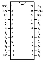
Pinout

  Connection Diagram


Specifications

Supply Voltage (VCC).................. −0.5V to +7.0V
DC Input Diode Current (IIK)
    VI = −0.5V ......................................... −20 mA
    VI = VCC + 0.5V................................. +20 mA
DC Input Voltage (VI) .........−0.5V to VCC + 0.5V
DC Output Diode Current (IOK)
    VO = −0.5V........................................  −20 mA
    VO = VCC + 0.5V +20 mA
DC Output Voltage (VO) ......−0.5V to VCC + 0.5V
DC Output Source
    or Sink Current (IO)............................ ±50 mA
DC VCC or Ground Current
    per Output Pin (ICC or IGND)............... ±50 mA
Storage Temperature (TSTG)... −65°C to +150°C

Junction Temperature (TJ)
    PDIP ......................................................140°C


Description

The 74AC648 consists of registered bus transceiver circuits, with outputs, D-type flip-flops and control circuitry providing multiplexed transmission of data directly from the input bus or from the internal storage registers. Data on the A or B bus will be loaded into the respective registers on the LOW-to-HIGH transition of the appropriate clock pin (CPAB or CPBA). The four fundamental data handling functions of the 74AC648 available are illustrated in Figure 1, Figure 2, Figure 3, and Figure 4.


Customers Who Bought This Item Also Bought

Margin,quality,low-cost products with low minimum orders. Secure your online payments with SeekIC Buyer Protection.
Circuit Protection
Boxes, Enclosures, Racks
Power Supplies - Board Mount
Test Equipment
View more