Features: Independent registers for A and B buses
Multiplexed real-time and stored data transfers
3-STATE outputs
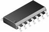
300 mil dual-in-line package
Outputs source/sink 24 mA
ACT646 has TTL compatible inputsPinout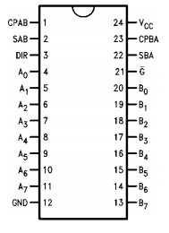 SpecificationsSupply Voltage (VCC).................. −0.5V to +7.0V
DC Input Diode Current (IIK)
VI= −0.5V......................................... −20 mA
VI= VCC + 0.5V................................. +20 mA
DC Input Voltage (VI) .........−0.5V to VCC + 0.5V
DC Output Diode Current (IOK)
VO = −0.5V........................................ −20 mA
VO = VCC + 0.5V +20 mA
DC Output Voltage (VO) ......−0.5V to VCC + 0.5V
DC Output Source
or Sink Current (IO)............................ ±50 mA
DC VCC or Ground Current
per Output Pin (ICC or IGND)............... ±50 mA
Storage Temperature (TSTG)... −65°C to +150°C
Junction Temperature (TJ)
PDIP ......................................................140°CDescriptionThe 74AC646 consist of registered bus transceiver circuits, with outputs, D-type flip-flops and control circuitry providing multiplexed transmission of data directly from the input bus or from the internal storage registers. Data on the A or B bus will be loaded into the respective registers on the LOW-to-HIGH transition of the appropriate clock pin (CPAB or CPBA). The four fundamental data handling functions available are illustrated in Figures 1, 2, 3, and Figure 4.
The 74AC646 includes registered bus transceiver circuits,with outputs,D-type flip-flops and control circuitry offering multiplexed transmission of data directly from the input bus or from the internal storage registers. Data on the A or B bus will be loaded into the respective registers on the LOW-to-HIGH transition of the appropriate clock pin(CPAB or CPBA).
Features of 74AC646 are:(1) independent registers for A and B buses; (2) multiplexed real-time and stored data tr-ansfers; (3) 3-STATE outputs; (4) 300 mil dual-in-line package; (5) outputs source/sink 24 mA; (6) ACT646 has TTL compatible inputs.
The absolute maximum ratings of the 74AC646 can be summarized as:(1):supply voltage is 0.5V to +7.0V;(2):DC in-put diode current is-20mA when VI is-0.5V,DC input diode current is+20mA when VI is VCC+0.5V;(3):DC input voltag e is 0.5V to VCC + 0.5V;(4):DC output diode current is-20mA when VO is-0.5V,DC output diode current is+20mA whe n VO isVCC+0.5V;(5):DC output voltage is-0.5V to VCC + 0.5V;(6):DC output source or sink current is±50 mA;(7):DC VCC or ground current is ±50 mA per output pin ;(8):storage temperature ranges from-65°C to +150°C;(9):junctio n temperature is 140.

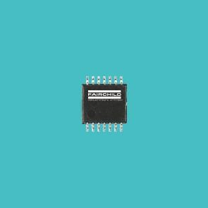
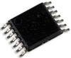
 74AC646 Data Sheet