DescriptionThe 74AC373 consists of eight latches with 3-STATE outputs for bus organized system applications. The 3-STATE standard outputs are controlled by the Output Enable (OE) input. When OE is LOW, the standard outputs are in the 2-state mode. When OE is HIGH, the standard outputs are in the h...
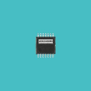
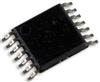
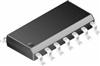
74AC373: DescriptionThe 74AC373 consists of eight latches with 3-STATE outputs for bus organized system applications. The 3-STATE standard outputs are controlled by the Output Enable (OE) input. When OE is L...
SeekIC Buyer Protection PLUS - newly updated for 2013!
268 Transactions
All payment methods are secure and covered by SeekIC Buyer Protection PLUS.
The 74AC373 consists of eight latches with 3-STATE outputs for bus organized system applications. The 3-STATE standard outputs are controlled by the Output Enable (OE) input. When OE is LOW, the standard outputs are in the 2-state mode. When OE is HIGH, the standard outputs are in the high impedance mode but this does not interfere with entering new data into the latches. The flip-flops appear transparent to the data when Latch Enable (LE) is HIGH. When LE is LOW, the data that meets the setup time is latched. Data appears on the bus when the Output Enable (OE) is LOW. When the Latch Enable (LE) input is HIGH, data on the Dn inputs enters the latches. In this condition the latches are transparent, i.e., a latch output will change state each time its D-type input changes. When OE is HIGH, the bus output is in the high impedance state. The 74AC373 contains eight D-type latches with 3-STATE standard outputs. When LE is LOW, the latches store the information that was present on the D-type inputs a setup time preceding the HIGH-to-LOW transition of LE.
The features of the 74AC373 can be summarized as (1)ICC and IOZ reduced by 50%; (2)eight latches in a single package; (3)3-STATE outputs for bus interfacing; (4)outputs source/sink 24 mA; (5)ACT373 has TTL-compatible inputs.
The absolute maximum ratings of the 74AC373 are (1)supply voltage (VCC): -0.5V to +7.0V; (2)DC input diode current (IIK) VI =-0.5V: -20 mA; VI = VCC + 0.5V: +20 mA; (3)DC input voltage (VI): -0.5V to VCC + 0.5V; (4)DC output diode current (IOK), VO =-0.5V: -20 mA; VO = VCC+ 0.5V: +20 mA; (5)DC output voltage (VO): -0.5V to VCC + 0.5V; (6)DC output source or Sink Current (IO): ± 50 mA; (7)DC VCC or ground current per output pin (ICC or IGND): ±50 mA; (8)storage temperature (TSTG): -65°C to +150°C; (9)junction temperature (TJ) PDIP:140°C.