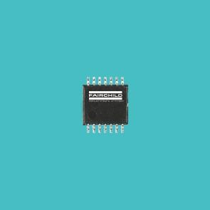
Features: ` Eight D-Type Flip-Flops in a Single Package
` 3-State Bus-Driving True Outputs
` Full Parallel Access for Loading
` Flow-Through Architecture Optimizes PCB Layout
` Center-Pin VCC and GND Configurations Minimize High-Speed Switching Noise
` EPICTM (Enhanced-Performance Implanted CMOS) 1-m Process
` 500-mA Typical Latch-Up Immunity at 125°C
` Package Options Include Plastic Small-Outline (DW) and Shrink Small-Outline (DB) Packages, and Standard
Plastic 300-mil DIPs (NT)
SpecificationsSupply voltage range, VCC . . . . . . . . . . . . . . . . . . . . . . . . . . . . . . . . . . . . . . . . . . . . . . . 0.5 V to 7 V
Input voltage range, VI (see Note 1) . . . . . . . . . . . . . . . . . . . . . . . . . . . . . . . . 0.5 V to VCC + 0.5 V
Output voltage range, VO (see Note 1) . . . . . . . . . . . . . . . . . . . . . . . . . . . . . . . 0.5 V to VCC + 0.5 V
Input clamp current, IIK (VI < 0 or VI > VCC) . . . . . . . . . . . . . . . . . . . . . . . . . . . . . . . . . . . . . . ±20 mA
Output clamp current, IOK (VO < 0 or VO > VCC) . . . . . . . . . . . . . . . . . . . . . . . . . . . . . . . . . . . ±50 mA
Continuous output current, IO (VO = 0 to VCC) . . . . . . . . . . . . . . . . . . . . . . . . . . . . . . . . . . . . ±50 mA
Continuous current through VCC or GND . . . . . . . . . . . . . . . . . . . . . . . . . . . . . . . . . . . . . . . . ±200 mA
Maximum power dissipation at TA = 55°C (in still air) (see Note 2): DB package . . . . . . . . . . . 0.65 W
DW package . . . . . . . . . . . . . . . . . . 1.7 W
NT package . . . . . . . . . . . . . . . . . . . 1.3 W
Storage temperature range, Tstg . . . . . . . . . . . . . . . . . . . . . . . . . . . . . . . . . . . . . . .65°C to 150°C
NOTES: 1. The input and output voltage ratings may be exceeded if the input and output current ratings are bserved.
2. The maximum package power dissipation is calculated using a junction temperature of 150�C and a board trace length of 750 mils, except for the NT package, which has a trace length of zero.
DescriptionThis 8-bit flip-flop features 3-state outputs of the 74AC11374 designed specifically for driving highly-capacitive or relatively low-impedance loads. It is particularly suitable for implementing buffer registers, I/O ports, bidirectional bus drivers, and working registers.
The eight flip-flops of the 74AC11374 are edge-triggered D-type flip-flops. On the positive transition of the clock, the Q outputs are set to the logic levels set up at the D inputs.
The output-enable (OE) input can be used to place the eight outputs in either a normal logic state (high or low logic levels) or a high-impedance state. In the high-impedance state, the outputs neither load nor drive the bus lines signigicantly. The high-impedance third state provides the capability to drive the bus lines in a bus-organized system without need for interface or pullup components.
OE does not affect the internal operation of the flip-flops. Old data can be retained or new data can be entered while the outputs are in the high-impedance state.
The 74AC11374 is characterized for operation from 40°C to 85°C.

 74AC11374 Data Sheet


