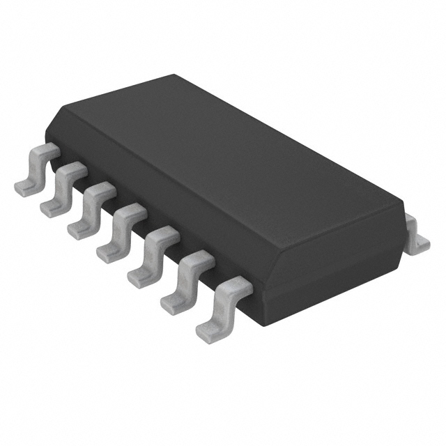
DescriptionThe 74ABT861PWDH is one member of the 74ABT861 series.The 74ABT861 bus transceiver provides high performance bus interface buffering for wide data/address paths of buses carrying parity.The 74ABT861 10-bit bus transceiver has NOR-ed transmit and receive output enables for maximum contro...
74ABT861PWDH: DescriptionThe 74ABT861PWDH is one member of the 74ABT861 series.The 74ABT861 bus transceiver provides high performance bus interface buffering for wide data/address paths of buses carrying parity.T...
SeekIC Buyer Protection PLUS - newly updated for 2013!
268 Transactions
All payment methods are secure and covered by SeekIC Buyer Protection PLUS.
The 74ABT861PWDH is one member of the 74ABT861 series.The 74ABT861 bus transceiver provides high performance bus interface buffering for wide data/address paths of buses carrying parity.The 74ABT861 10-bit bus transceiver has NOR-ed transmit and receive output enables for maximum control flexibility.
Features of the 74ABT861PWDH are:(1)provides high performance bus interface buffering for wide data/address paths or buses carrying parity; (2)buffered control inputs for light loading, or increased fan-in as required with MOS microprocessors; (3)output capability: +64mA/32mA; (4)latch-up protection exceeds 500mA per Jedec Std 17; (5)ESD protection exceeds 2000 V per MIL STD 883 Method 3015 and 200 V per Machine Model; (6)power-up 3-State; (7)inputs are disabled during 3-State mode.Limiting values given are in accordance with the Absolute Maximum Rating System (IEC 134). Stress above one or more of the limiting values may cause permanent damage to the device. These are stress ratings only and operation of the device at these or at any other conditions above those given in the Characteristics sections of the specification is not implied. Exposure to limiting values for extended periods may affect device reliability.
The absolute maximum ratings of the 74ABT861PWDH can be summarized as:(1)DC supply voltage:-0.5 to 7.0V;(2)DC input voltage:-1.2 to 7.0V;(3)DC output voltage:-0.5 to 5.5V;(4)DC input diode current:-18mA; (5)DC output diode current:-50mA; (6)DC output current:128mA; (7)storage temperature range:-65 to 150.Stresses beyond those listed may cause permanent damage to the device. These are stress ratings only and functional operation of the device at these or any other conditions beyond those indicated under "recommended operating conditions" is not implied. Exposure to absolute-maximum-rated conditions for extended periods may affect device reliability.These products are not designed for use in life support appliances, devices or systems where malfunction of these products can reasonably be expected to result in personal injury. Philips Semiconductors customers using or selling these products for use in such applications do so at their own risk and agree to fully indemnify Philips Semiconductors for any damages resulting from such application.