74ABT843D

DescriptionThe 74ABT843D belongs to 74ABT843 family. The bus interface latch is designed to eliminate the extra packages required to buffer existing registers and provide extra data width for wider data/address paths of buses carrying parity. The 74ABT843 consists of nine D-type latches with 3-Sta...

product image

74ABT843D Picture
SeekIC No. : 004248777 Detail

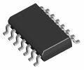
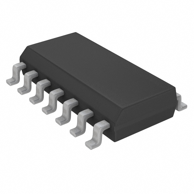
74ABT843D: DescriptionThe 74ABT843D belongs to 74ABT843 family. The bus interface latch is designed to eliminate the extra packages required to buffer existing registers and provide extra data width for wider ...

floor Price/Ceiling Price

Part Number:
74ABT843D
Supply Ability:
5000

Price Break

  • Qty
  • 1~5000
  • Unit Price
  • Negotiable
  • Processing time
  • 15 Days
Total Cost: $ 0.00

SeekIC Buyer Protection PLUS - newly updated for 2013!

  • Escrow Protection.
  • Guaranteed refunds.
  • Secure payments.
  • Learn more >>

Month Sales

268 Transactions

Rating

evaluate  (4.8 stars)

Upload time: 2024/5/18

Payment Methods

All payment methods are secure and covered by SeekIC Buyer Protection PLUS.

Notice: When you place an order, your payment is made to SeekIC and not to your seller. SeekIC only pays the seller after confirming you have received your order. We will also never share your payment details with your seller.
Product Details

Description


Description

The 74ABT843D belongs to 74ABT843 family. The bus interface latch is designed to eliminate the extra packages required to buffer existing registers and provide extra data width for wider data/address paths of buses carrying parity. The 74ABT843 consists of nine D-type latches with 3-State outputs. In addition to the LE and OE pins, it has a Master Reset (MR) pin and Preset (PRE) pin. These pins are ideal for parity bus interfacing in high performance systems. When MR is Low, the outputs are Low if OE is Low. When MR is High, data can be entered into the latch. When PRE is Low, the outputs are High, if OE is Low. PRE overrides MR.

The features of 74ABT843D can be summarized as (1)high speed parallel latches; (2)extra data width for wide address/data paths or buses carrying parity; (3)ideal where high speed, light loading, or increased fan-in are required with MOS microprocessors; (4)slim DIP 300 mil package; (5)broadside pinout; (6)output capability: +64mA/±32mA; (7)latch-up protection exceeds 500mA per Jedec Std 17; (8)ESD protection exceeds 2000V per MIL STD 883 Method 3015 and 200V per Machine Model; (9)power-up 3-state; (10)power-up reset.

The absolute maximum ratings of 74ABT843D are (1)VCC DC supply voltage: -0.5 to +7.0V; (2)VI input voltage range: -1.2 to +7.0V; (3)IIK DC input diode current(VI < 0): -18mA; (4)IOK DC output diode current(VO <0): -50mA; (5)IOUT DC output current(output in Low state): 128mA; (6)VOUT DC output voltage (output in off or high state): -0.5 to +5.5V; (7)Tstg storage temperature range: -65 to +150°C.(1. Stresses beyond those listed may cause permanent damage to the device. These are stress ratings only and functional operation of the device at these or any other conditions beyond those indicated under arecommended operating conditionso is not implied. Exposure to absolute-maximum-rated conditions for extended periods may affect device reliability. 2. The performance capability of a high-performance integrated circuit in conjunction with its thermal environment can create junction temperatures which are detrimental to reliability. The maximum junction temperature of this integrated circuit should not exceed 150°C. 3. The input and output voltage ratings of the 74ABT843D may be exceeded if the input and output current ratings are observed.)


Customers Who Bought This Item Also Bought

Margin,quality,low-cost products with low minimum orders. Secure your online payments with SeekIC Buyer Protection.
Memory Cards, Modules
Industrial Controls, Meters
Discrete Semiconductor Products
Audio Products
Boxes, Enclosures, Racks
View more