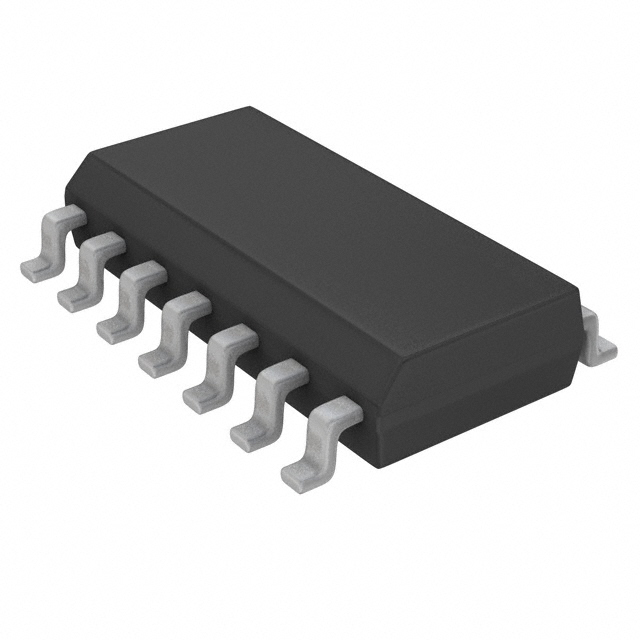
DescriptionThe 74ABT841PWDH is one member of the 74ABT841 series.The 74ABT841 bus interface register is designed to provide extra data width for wider data/address paths of buses carrying parity.The 74ABT841 consists of ten D-type latches with 3-State outputs.The flip-flops appear transparent to the data when Latch Enable(LE) is High. This allows asynchronous operation, as the output transition follows the data in transition. On the LE High-to-Low transition, the data that meets the setup and hold time is latched.Data appears on the bus when the Output Enable (OE) is Low.When OE is High the output is in the High-impedance state.
Features of the 74ABT841PWDH are:(1)high speed parallel latches; (2)extra data width for wide address/data paths or buses carrying parity; (3)ideal where high speed, light loading, or increased fan-in are required with mos microprocessors; (4)slim DIP 300 mil package; (5)broadside pinout; (6)output capability: +64mA/32mA; (7)latch-up protection exceeds 500mA per Jedec Std 17; (8)ESD protection exceeds 2000 V per MIL STD 883 Method 3015 and 200 V per Machine Model; (9)power-up 3-state; (10)power-up reset.
The absolute maximum ratings of the 74ABT841PWDH can be summarized as:(1)DC supply voltage:-0.5 to 7.0V;(2)DC input voltage:-1.2 to 7.0V;(3)DC output voltage:-0.5 to 5.5V;(4)DC input diode current:-18mA; (5)DC output diode current:-50mA; (6)DC output current:128mA; (7)storage temperature range:-65 to 150.Stresses beyond those listed may cause permanent damage to the device. These are stress ratings only and functional operation of the device at these or any other conditions beyond those indicated under "recommended operating conditions" is not implied. Exposure to absolute-maximum-rated conditions for extended periods may affect device reliability.The products described in this document are designed, developed and manufactured as contemplated for general use, including without limitation, ordinary industrial use, general office use, personal use, and household use, but are not designed, developed and manufactured as contemplated (1) for any use that includes fatal risks or dangers that, unless extremely high safety is secured, could have a serious effect to the public, and could lead directly to death, personal injury, severe physical damage or other loss (i.e., nuclear reaction control in nuclear facility, aircraft flight control, air traffic control, mass transport control, medical life support system, missile launch control of the 74ABT841PWDH in weapon system), or (2) for any use where chance of failure is intolerable (i.e., submersible repeater and artificial satellite).

 74ABT841PWDH Data Sheet


