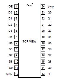
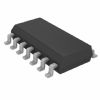
Features: • High speed parallel latches• Extra data width for wide address/data paths or buses carrying parity• Ideal where high speed, light loading, or increased fan-in are required with MOS microprocessors• Slim DIP 300 mil package• Broadside pinout• Output c...
74ABT841: Features: • High speed parallel latches• Extra data width for wide address/data paths or buses carrying parity• Ideal where high speed, light loading, or increased fan-in are requi...
SeekIC Buyer Protection PLUS - newly updated for 2013!
268 Transactions
All payment methods are secure and covered by SeekIC Buyer Protection PLUS.
SYMBOL | PARAMETER | CONDITIONS | RATING | UNIT |
VCC | DC supply voltage | 0.5 to +7.0 | V | |
IIK | DC input diode current | VI < 0 | 18 | mA |
VI | DC input voltage3 | 1.2 to +7.0 | V | |
IOK | DC output diode current | VO < 0 | 50 | mA |
VOUT | DC output voltage3 | output in Off or High state | 0.5 to +5.5 | V |
IOUT | DC output current | output in Low state | 128 | mA |
Tstg | Storage temperature range | 65 to 150 | °C |
NOTES:
1. Stresses beyond those listed may cause permanent damage to the device. These are stress ratings only and functional operation of the device at these or any other conditions beyond those indicated under "recommended operating conditions" is not implied. Exposure to absolute-maximum-rated conditions for extended periods may affect device reliability.
2. The performance capability of a high-performance integrated circuit in conjunction with its thermal environment can create junction temperatures which are detrimental to reliability. The maximum junction temperature of this integrated circuit should not exceed 150°C.
3. The input and output voltage ratings may be exceeded if the input and output current ratings are observed.
The 74ABT841 Bus interface register is designed to provide extra data width for wider data/address paths of buses carrying parity.
The 74ABT841 consists of ten D-type latches with 3-State outputs. The flip-flops appear transparent to the data when Latch Enable (LE) is High. This allows asynchronous operation, as the output transition follows the data in transition. On the LE High-to-Low transition, the data that meets the setup and hold time is latched.
Data appears on the bus when the Output Enable (OE) is Low. When OE is High the output is in the High-impedance state.