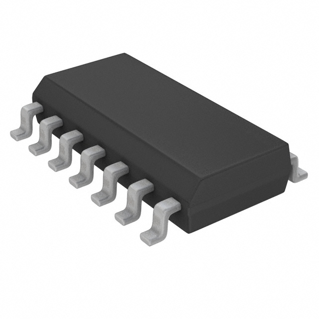
DescriptionThe 74ABT833N belongs to 74ABT833 family which is an octal transceiver with a parity generator/checker and is intended for bus-oriented applications. When Output Enable A (OEA) is High, it will place the A outputs in a high impedance state. Output Enable B (OEB) controls the B outputs i...
74ABT833N: DescriptionThe 74ABT833N belongs to 74ABT833 family which is an octal transceiver with a parity generator/checker and is intended for bus-oriented applications. When Output Enable A (OEA) is High, i...
SeekIC Buyer Protection PLUS - newly updated for 2013!
268 Transactions
All payment methods are secure and covered by SeekIC Buyer Protection PLUS.
The 74ABT833N belongs to 74ABT833 family which is an octal transceiver with a parity generator/checker and is intended for bus-oriented applications. When Output Enable A (OEA) is High, it will place the A outputs in a high impedance state. Output Enable B (OEB) controls the B outputs in the same way. The 74ABT833 high-performance BiCMOS device combines low static and dynamic power dissipation with high speed and high output drive. The parity generator creates an odd parity output (PARITY) when OEB is Low. When OEA is Low, the parity of the B port, including the PARITY input, is checked for odd parity. When an error is detected, the error data is sent to the input of a storage register. If a Low-to-High transition happens at the clock input (CP), the error data is stored in the register and the Open-collector error flag (ERROR) will go Low. The error flag register is cleared with a Low pulse on the CLEAR input. If both OEA and OEB are Low, data will flow from the A bus to the B bus and the part is forced into an error condition which creates an inverted PARITY output. This error condition of the 74ABT833N can be used by the designer for system diagnostics.
The features of 74ABT833N can be summarized as (1)low static and dynamic power dissipation with high speed and high output drive; (2)open-collector ERROR output with flag register; (3)output capability: +64mA/±32mA; (4)latch-up protection exceeds 500mA per Jedec Std 17; (5)ESD protection exceeds 2000V per MIL STD 883 Method 3015 and 200 V per machine model; (6)power up/down 3-State; (7)live insertion/extraction permitted.
The absolute maximum ratings of 74ABT833N are (1)VCC DC supply voltage: -0.5 to +7.0 V; (2)IIK DC input diode current(VI < 0): -18mA; (3)IOK DC output diode current:-50mA; (4)VI DC input voltage3: -1.2 to +7.0V; (5)VOUT DC output voltage3(output in Off or High state): -0.5 to +5.5V(6)Tstg storage temperature range: -65 to +150 °C; (7)IOUT DC output current(output in Low state): 128 mA.(NOTES:1. Stresses beyond those listed may cause permanent damage to the device. These are stress ratings only and functional operation of the device at these or any other conditions beyond those indicated under arecommended operating conditionso is not implied. Exposure to absolute-maximum-rated conditions for extended periods may affect device reliability. 2. The performance capability of a high-performance integrated circuit in conjunction with its thermal environment can create junction temperatures which are detrimental to reliability. The maximum junction temperature of this integrated circuit should not exceed 150°C. 3. The input and output voltage ratings of the 74ABT833N may be exceeded if the input and output current ratings are observed.).