Features: • Combinational functions in one package
• Low static and dynamic power dissipation with high speed and high output drive
• Output capability: +64mA/32mA
• Power-up 3-State
• Latch-up protection exceeds 500mA per Jedec Std 17
• ESD protection exceeds 2000 V per MIL STD 883 Method 3015 and 200 V per Machine ModelApplicationPhilips Semiconductors and Philips Electronics North America Corporation Products are not designed for use in life support appliances, devices, or systems where malfunction of a Philips Semiconductors and Philips Electronics North America Corporation Product can reasonably be expected to result in a personal injury. Philips Semiconductors and Philips Electronics North America Corporation customers using or selling Philips Semiconductors and Philips Electronics North America Corporation Products for use in such applications do so at their own risk and agree to fully indemnify Philips Semiconductors and Philips Electronics North America Corporation for any damages resulting from such improper use or sale.
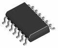
Pinout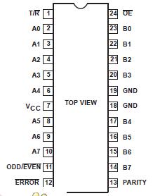 Specifications
| SYMBOL |
PARAMETER |
CONDITIONS |
RATING |
UNIT |
| VCC |
DC supply voltage |
|
0.5 to +7.0 |
V |
| IIK |
DC input diode current |
VI < 0 |
18 |
mA |
| VI |
DC input voltage3 |
|
1.2 to +7.0 |
V |
| IOK |
DC output diode current |
VO < 0 |
50 |
mA |
| VOUT |
DC output voltage3 |
output in Off or High state |
0.5 to +5.5 |
V |
| IOUT |
DC output current |
output in Low state |
128 |
mA |
| Tstg |
Storage temperature range |
|
65 to 150 |
°C |
NOTES:
1. Stresses beyond those listed may cause permanent damage to the device. These are stress ratings only and functional operation of the device at these or any other conditions beyond those indicated under "recommended operating conditions" is not implied. Exposure to absolute-maximum-rated conditions for extended periods may affect device reliability.
2. The performance capability of a high-performance integrated circuit in conjunction with its thermal environment can create junction temperatures which are detrimental to reliability. The maximum junction temperature of this integrated circuit should not exceed 150°C.
3. The input and output voltage ratings may be exceeded if the input and output current ratings are observed.
DescriptionThe 74ABT657 high-performance BiCMOS device combines low static and dynamic power dissipation with high speed and high output drive.
The 74ABT657 is an octal transceiver featuring non-inverting buffers with 3-State outputs and an 8-bit parity generator/checker, and is intended for bus-oriented applications. The buffers have a guaranteed current sinking capability of 64mA. The Transmit/Receive (T/R) input determines the direction of the data flow through the bidirectional transceivers. Transmit (active-High) enables data from A ports to B ports; Receive (active-Low) enables data from B ports to A ports.
The Output Enable (OE) input disables of the 74ABT657 both the A and B ports by placing them in a high impedance condition when the OE input is High. The parity select (ODD/EVEN) input gives the user the option of odd or even parity systems. The parity (PARITY) pin is an output from the generator/checker when transmitting from the port A to B (T/R = High) and an input when receiving from port B to A port (T/R = Low). When transmitting (T/R = High) the parity select (ODD/EVEN) input is set, then the A port data is polled to determine the number of High bits. The parity (PARITY) output then goes to the logic state determined by the parity select (ODD/EVEN) setting and by the number of High bits on port A. For example, if the parity select (ODD/EVEN) is set Low (even parity), and the number of High bits on port A is odd, then the parity (PARITY) output will be High, transmitting even parity. If the number of High bits on port A is even, then the parity (PARITY) output will be Low, keeping even parity. When in receive mode (T/R = Low) the B port is polled to determine the number of High bits. If parity select (ODD/EVEN) is Low (even parity) and the number of Highs on port B is:
(1) odd and the parity (PARITY) input is High, then ERROR will be High, signifying no error.
(2) even and the parity (PARITY) input is High, then ERROR will be asserted Low, indicating an error.

 74ABT657 Data Sheet