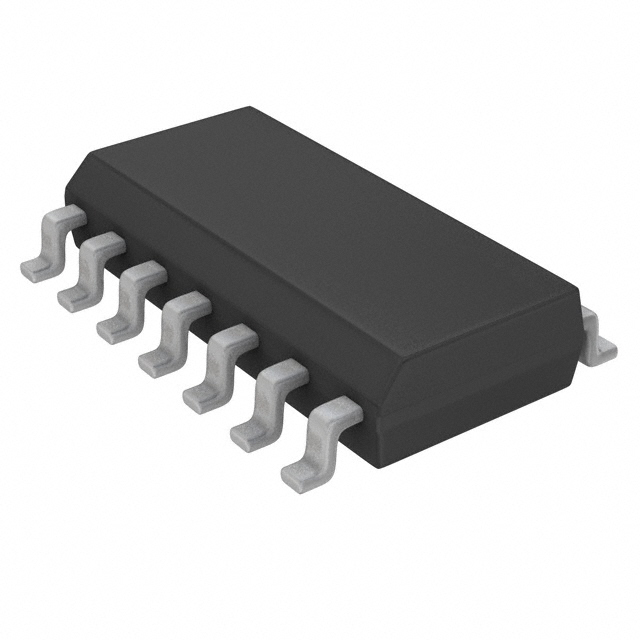
Number of Channels per Chip
: 8
Output Type
: 3-State
Packaging
: Tube
Supply Voltage - Max
: 5.5 V
Maximum Operating Temperature
: + 85 C
Supply Voltage - Min
: 4.5 V
Input Level
: TTL
Output Level
: TTL
Logic Family
: ABT
High Level Output Current
: - 32 mA
Low Level Output Current
: 64 mA
Logic Type
: BiCMOS
Propagation Delay Time
: 5.1 ns
Package / Case
: SO-24
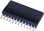
DescriptionThe 74ABT652AD consists of bus transceiver circuits with Dtype flip-flops and control circuitry arranged for multiplexed transmission of data directly from the input bus or from the internal registers. The feature of 74ABT652AD are as follows: (1)Independent registers for A and B buses; (2)Multiplexed real-time and stored data; (3)A and B output sink capability of 64 mA, source capability of 32 mA; (4)Guaranteed output skew; (5)Guaranteed multiple output switching specifications; (6)Output switching specified for both 50 pF and 250 pF loads; (7)Guaranteed simultaneous switching noise level and dynamic threshold performance; (8)Guaranteed latchup protection; (9)High impedance glitch free bus loading during entire power up and power down cycle; (10)Nondestructive hot insertion capability.
The absolute maximum ratings of the 74ABT652AD are: (1)storage temperature: -65°C to +150°C; (2)ambient temperature under bias: -55°C to +125°C; (3)junction temperature under bias: -55°C to +150°C; (4)VCC pin potential to ground pin: -0.5V to +7.0V; (5)input voltage: -0.5V to +7.0V; (6)input current: -30 mA to +5.0 mA; (7)voltage applied to any output in the disable or power-off state -0.5V to +5.5V, in the HIGH state -0.5V to VCC; (8)current applied to output in LOW state (Max) twice the rated IOL (mA); (9)DC latchup source current: -500 mA; (10)over voltage latchup (I/O): 10V.
The following is about the electrical characteristics of 74ABT652AD: (1)input high voltage: 2.0 V min at recognized high signal; (2)input low voltage: 0.8 V max at recognized low signal; (3)input clamp diode voltage: -1.2 V Min at IIN = -18 mA (Non I/O Pins); (4)output high voltage: 2.5 V min at IOH = -3 mA, (An, Bn); (5)output low voltage: 0.55 V min at IOL = 64 mA, (An, Bn); (6)input leakage test: 4.75 V min at IID = 1.9 mA, (Non-I/O Pins), all other pins grounded; (7)input high current: 1 mA Max at VIN = 2.7V (Non-I/O Pins); (8)input high current breakdown test: 7 mA Max at VIN = 7.0V (Non-I/O Pins); (9)input high current breakdown test (I/O): 100 mA Max at VIN = 5.5V (An, Bn); (10)input low current: -1 mA max at VIN = 0.5V (Non-I/O Pins).
 74ABT652AD Data Sheet
