Features: • Independent registers for A and B buses• The 74ABT651 is the inverting version of the 74ABT652• Multiplexed real-time and stored data• 3-State outputs• Live insertion/extraction permitted.• Power-up 3-State• Power-up reset• Output capabil...
74ABT651: Features: • Independent registers for A and B buses• The 74ABT651 is the inverting version of the 74ABT652• Multiplexed real-time and stored data• 3-State outputs• Live...
SeekIC Buyer Protection PLUS - newly updated for 2013!
268 Transactions
All payment methods are secure and covered by SeekIC Buyer Protection PLUS.
SYMBOL | PARAMETER |
CONDITIONS |
RATING |
UNIT |
VCC | DC supply voltage |
0.5 to +0.7 |
V | |
IIK | DC input diode current |
VI < 0 |
18 |
mA |
VI | DC input voltage3 |
1.2 to +7.0 |
V | |
IOK | DC output diode current |
VO < 0 |
50 |
mA |
VOUT | DC output voltage3 |
Output in Off |
0.5 to +5.5 |
V |
IOUT | DC output current |
Output in Low state |
128 |
mA |
Tstg | Storage temperature range |
65 to +150 |
°C |
NOTES:
1. Stresses beyond those listed may cause permanent damage to the device. These are stress ratings only and functional operation of the device at these or any other conditions beyond those indicated under "recommended operating conditions" is not implied. Exposure to absolute-maximum-rated conditions for extended periods may affect device reliability.
2. The performance capability of a high-performance integrated circuit in conjunction with its thermal environment can create junction temperatures which are detrimental to reliability. The maximum junction temperature of this integrated circuit should not exceed 150°C.
3. The input and output negative voltage ratings may be exceeded if the input and output clamp current ratings are observed.
The 74ABT651 high-performance BiCMOS device combines low static and dynamic power dissipation with high speed and high output drive.
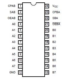
The 74ABT651 transceiver/register consists of bus transceiver circuits with 3-State outputs, D-type flip-flops, and control circuitry arranged for multiplexed transmission of data directly from the input bus or the internal registers. Data on the A or B bus will be clocked into the registers as the appropriate clock pin goes High. Output Enable (OEAB, OEBA) and Select (SAB, SBA) pins are provided for bus management.
The following examples demonstrate the four fundamental bus-management functions that can be performed with the 74ABT651.
The select pins determine whether data is stored or transferred through the device in real time. The output enable pins determine the direction of the data flow.