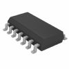
Features: • Combines 74ABT245 and 74ABT374 type functions in one device• Independent registers for A and B buses• Multiplexed real-time and stored data• Output capability: +64mA/32mA• Power-up 3-state• Power-up reset• Live insertion/extraction permitted...
74ABT648: Features: • Combines 74ABT245 and 74ABT374 type functions in one device• Independent registers for A and B buses• Multiplexed real-time and stored data• Output capability: +6...
SeekIC Buyer Protection PLUS - newly updated for 2013!
268 Transactions
All payment methods are secure and covered by SeekIC Buyer Protection PLUS.
SYMBOL | PARAMETER | CONDITIONS | RATING | UNIT |
VCC | DC supply voltage | 0.5 to +7.0 | V | |
IIK | DC input diode current | VI < 0 | 18 | mA |
VI | DC input voltage3 | 1.2 to +7.0 | V | |
IOK | DC output diode current | VO < 0 | 50 | mA |
VOUT | DC output voltage3 | output in Off or High state | 0.5 to +5.5 | V |
IOUT | DC output current | output in Low state | 128 | mA |
Tstg | Storage temperature range | 65 to 150 | °C |
NOTES:
1. Stresses beyond those listed may cause permanent damage to the device. These are stress ratings only and functional operation of the device at these or any other conditions beyond those indicated under "recommended operating conditions" is not implied. Exposure to absolute-maximum-rated conditions for extended periods may affect device reliability.
2. The performance capability of a high-performance integrated circuit in conjunction with its thermal environment can create junction temperatures which are detrimental to reliability. The maximum junction temperature of this integrated circuit should not exceed 150°C.
3. The input and output voltage ratings may be exceeded if the input and output current ratings are observed.
The 74ABT648 high-performance BiCMOS device combines low static and dynamic power dissipation with high speed and high output drive.
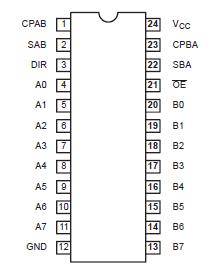
The 74ABT648 transceiver/register consists of bus transceiver circuits with inverting 3-State outputs, D-type flip-flops, and control circuitry arranged for multiplexed transmission of data directly from the input bus or the internal registers. Data on the A or B bus will be clocked into the registers as the appropriate clock pin goes High. Output Enable (OE) and DIR pins are provided to control the transceiver function. In the transceiver mode, data present at the high impedance port may be stored in either the A or B register or both.
The Select (SAB, SBA) pins of the 74ABT648 determine whether data is stored or transferred through the device in realtime. The DIR determines which bus will receive data when the OE is active (Low). In the isolation mode (OE = High), data from Bus A may be stored in the B register and/or data from Bus B may be stored in the A register. Outputs from real-time, or stored registers will be inverted. When an output function is disabled, the input function is still enabled and may be used to store and transmit data. Only one of the two buses, A or B may be driven at a time. The examples on the next page demonstrate the four fundamental bus management functions that can be performed with the 74ABT648.